A kind of manufacturing method of pcb board

A technology of PCB board and manufacturing method, which is applied in the direction of multilayer circuit manufacturing and printed circuit components, etc., can solve the problems of poor product quality, slow production progress, low stacking efficiency, etc., and achieve the effect of reducing technical difficulties and being easy to realize

Active Publication Date: 2015-11-25
NEW FOUNDER HLDG DEV LLC +1
View PDF3 Cites 0 Cited by
  • Summary
  • Abstract
  • Description
  • Claims
  • Application Information

AI Technical Summary

Problems solved by technology

[0008] In order to solve the problems of large stacking workload, low stacking efficiency, slow production progress, and poor product quality caused by flipping the stacked boards during the stacking process of local mixed pressure and copper block blind buried boards, the present invention provides a PCB board Manufacturing method and PCB board

Method used


Image

  • A kind of manufacturing method of pcb board
  • A kind of manufacturing method of pcb board
  • A kind of manufacturing method of pcb board

Examples


Embodiment Construction

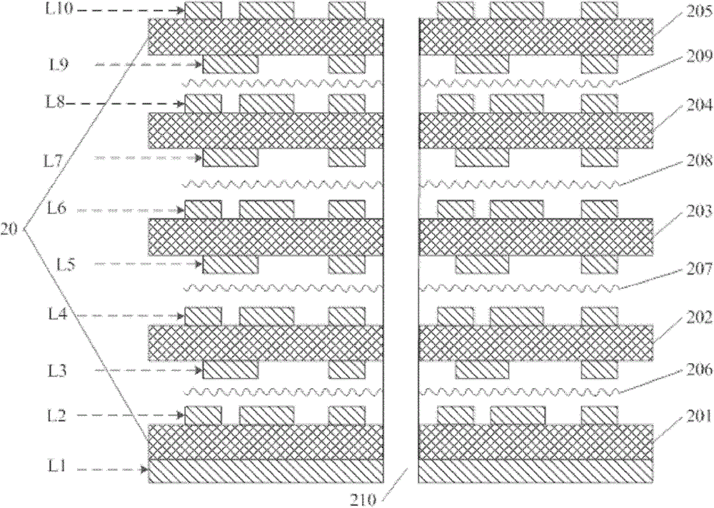
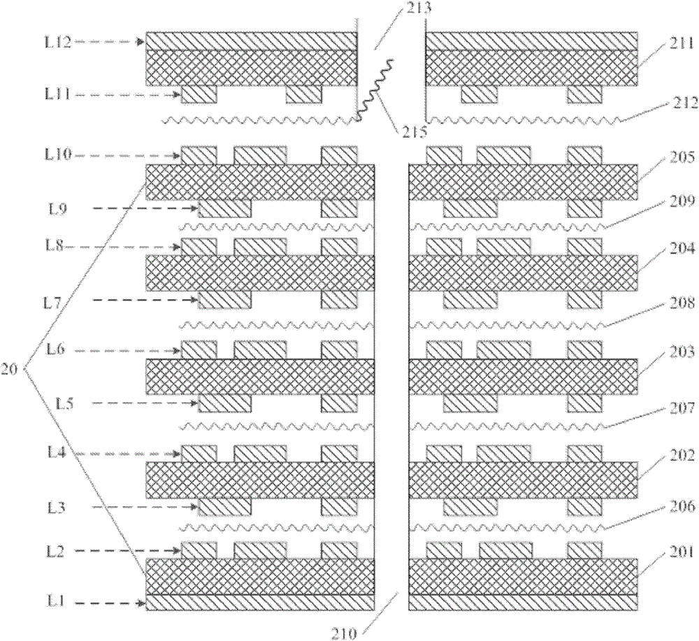
[0029] An embodiment of the present invention provides a method for manufacturing a PCB board, which is used to manufacture a PCB board including a partial mixed voltage sub-board and a heat dissipation copper block. In this embodiment, please refer to figure 1 , the PCB board is illustrated by taking a 12-layer (ie 12L) partially mixed-pressed copper block blind buried board as an example. The PCB board includes a stack 20, and the stack 20 includes a first sub-core board 201, and the first sub-core board 201 includes a layer Insulation layer and double-sided copper lines L1, L2; second sub-core board 202, including a layer of insulation layer and double-sided copper lines L3, L4; third sub-core board 203, including a layer of insulation layer and double-sided copper lines L5 , L6; the fourth sub-core board 204, including a layer of insulating layer and double-sided copper lines L7, L8; the fifth sub-core board 205, including a layer of insulating layer and double-sided copper...


PUM


Abstract

The invention discloses a manufacturing method for a printed circuit board (PCB) and the PCB. The method comprises the steps that a first window is formed in first core plates and first resin plates, wherein the first core plates and the first resin plates form a lamination, and the shape and the size of the first window are matched with the shape and the size of a heat dissipation copper block; a second window is formed in second core plates and second resin plates between the second core plates and the lamination, wherein a daughter plate is to be inserted into the second core plates, and resin blocks at the position of the second window of the second resin plates are enabled to be connected with one edge of the second window of the second resin plates, wherein the shape and the size of the second window are matched with the shape and the size of the daughter plate; sol dissolving is conducted on the lamination, the second core plates and the second resin plates; the resin blocks at the position of the second window of the second resin plate are turned over, and the heat dissipation copper block is embedded into the first window in the lamination through the second window; the resin blocks at the position of the second window of the second resin plate are dissolved into the second window of the second resin plates; and the daughter plate is embedded into the second window of the second core plates.

Description

technical field [0001] The invention relates to the field of printed circuit board processing, in particular to a method for manufacturing a PCB board and the PCB board. Background technique [0002] With the high-frequency development of electronic equipment, especially the development of wireless networks and satellite communication equipment, information products are moving towards high speed and high frequency, and communication products are moving towards large capacity and fast wireless transmission of voice, video and data standardization development trend is inevitable. The substrates required by the new generation of communication products also need to cooperate with its development, and obviously the traditional FR-4 materials cannot meet the existing needs. If high-frequency signals are to be used in the traditional PCB production process, the entire layer is designed to be made of high-frequency materials. If only partial (mostly less than 1 / 3 of the entire boar...

Claims


Application Information

Patent Timeline
Patent Type & Authority Patents(China)
IPC IPC(8): H05K3/46H05K1/02
Inventor 华炎生
Owner NEW FOUNDER HLDG DEV LLC
Why Eureka
Try Eureka