Very high bandwidth germanium-silicon photoelectric detector

A photodetector and bandwidth technology, which is applied in the direction of circuits, electrical components, semiconductor devices, etc., can solve the problem of low working bandwidth of parasitic parameters

Inactive Publication Date: 2015-09-30
HUAZHONG UNIV OF SCI & TECH
View PDF4 Cites 4 Cited by
  • Summary
  • Abstract
  • Description
  • Claims
  • Application Information

AI Technical Summary

Problems solved by technology

[0004] The problem to be solved by the present invention is to provide an ultra-high bandwidth silicon-germanium photodetector to overcome the problem that the existing silicon-germanium photodetector is limited by various parasitic parameters and has a relatively low working bandwidth

Method used


Image

  • Very high bandwidth germanium-silicon photoelectric detector
  • Very high bandwidth germanium-silicon photoelectric detector
  • Very high bandwidth germanium-silicon photoelectric detector

Examples


Embodiment Construction

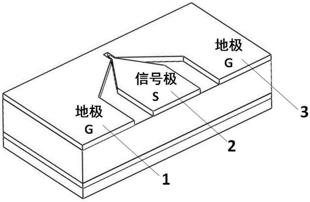
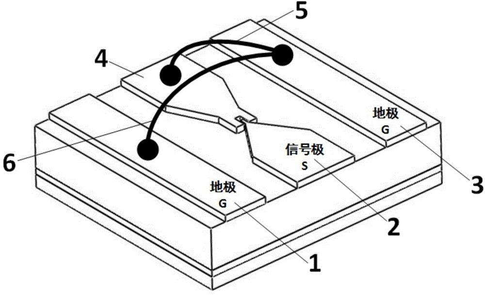
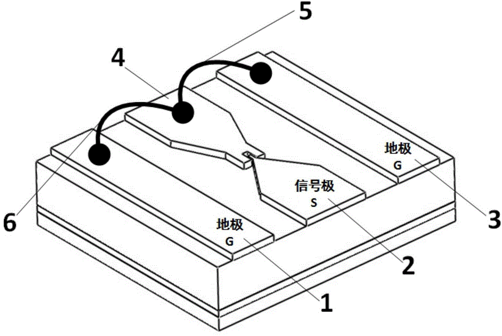
[0032] Such as figure 2 Shown is a structural schematic diagram of a specific embodiment of the ultra-high bandwidth silicon germanium photodetector of the present invention. The working principle, implementation conditions and steps of the present invention will be described in detail below in conjunction with related device structure diagrams.

[0033] The invention utilizes the Wire Bonding technology to introduce one or several sections of wires between several ground electrodes that are physically isolated from each other in the electrode of the germanium-silicon photodetector, and uses the total inductance formed by the wires to offset the charging and discharging of the device at high frequency process, thereby increasing device bandwidth.

[0034] The wire can be made of gold wire, silver wire, copper wire, etc., which can meet the requirements of the Wire Bonding packaging process. In this specific implementation manner, a gold wire is taken as an example for furth...


PUM


Abstract

The invention relates to a silicon-based integrated optoelectronic device, a very high bandwidth germanium-silicon photoelectric detector, for high-speed high-capacity fiber communication systems. The very high bandwidth germanium-silicon photoelectric detector comprises a plurality of ground electrodes physically separated and a signal electrode; the ground electrodes are connected through one or a plurality of wires; total inductance of the wire or the multiple wires ranges from 50 pH to 900 pH. The wires of certain inductance are introduced to the electrodes of the existing germanium-silicon photoelectric detector by means of wire bonding, and a bandwidth curve of the detector has a certain rise at the high-frequency part. The very high bandwidth germanium-silicon photoelectric detector is achieved without increasing the process complexity or affecting other performance parameters of the detector.

Description

technical field [0001] The invention relates to a silicon-based integrated optoelectronic device in a high-speed and large-capacity optical fiber communication system, in particular to a high-speed germanium-silicon photoelectric detector. Background technique [0002] With the explosive growth of global information data volume, higher and higher requirements are put forward for high-speed optical fiber communication system. The application of various advanced modulation formats and multi-dimensional multiplexing methods has greatly improved the transmission rate and transmission capacity of the optical fiber communication system. As the rate of optical fiber communication systems is getting higher and higher, if you continue to use traditional discrete components, factors such as power consumption and cost determine that this is very unrealistic. Therefore, the development of integrated optoelectronic devices is an inevitable trend. Among various integrated platforms, sil...

Claims


Application Information

Patent Timeline
IPC IPC(8): H01L31/02
CPCH01L31/02005
Inventor 余宇陈冠宇张新亮
Owner HUAZHONG UNIV OF SCI & TECH
Why Eureka
Try Eureka