Substrate of electronic device and preparation method therefor

A technology for electronic devices and substrates, which is applied to the substrates of electronic devices and their preparation fields, can solve problems such as the surface effect of the substrate being flat and rigid, and achieve the effects of rich visual effects and stereoscopic visual effects.

Inactive Publication Date: 2016-01-27
VIVO MOBILE COMM CO LTD
View PDF4 Cites 8 Cited by
  • Summary
  • Abstract
  • Description
  • Claims
  • Application Information

AI Technical Summary

Problems solved by technology

[0004] Embodiments of the present invention provide a substrate of an electronic device and a preparation method thereof, to solve the problem that the surface effect plane of the substrate of an electronic device is hard in the prior art

Method used


Image

  • Substrate of electronic device and preparation method therefor
  • Substrate of electronic device and preparation method therefor
  • Substrate of electronic device and preparation method therefor

Examples


Embodiment Construction

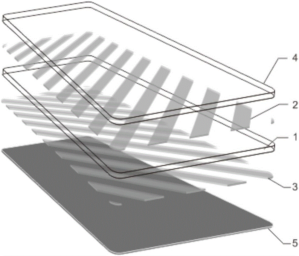
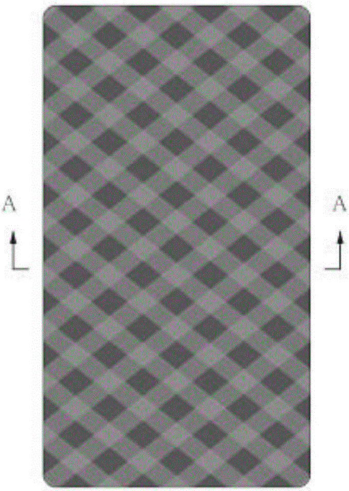
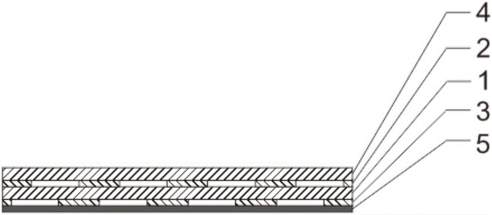
[0034] In order to make the technical problems, technical solutions and beneficial effects solved by the present invention clearer, the present invention will be further described in detail below in conjunction with the accompanying drawings and embodiments. It should be understood that the specific embodiments described here are only used to explain the present invention, not to limit the present invention.

[0035] In describing the present invention, it is to be understood that the terms "longitudinal", "radial", "length", "width", "thickness", "upper", "lower", "front", "rear", The orientation or positional relationship indicated by "left", "right", "vertical", "horizontal", "top", "bottom", "inner", "outer" etc. is based on the orientation or positional relationship shown in the drawings, It is only for the convenience of describing the present invention and simplifying the description, but does not indicate or imply that the device or element referred to must have a spec...


PUM


Abstract

The invention discloses a substrate of an electronic device. The substrate comprises a first transparent sheet material layer, a first light transmission hollow layer and a second light transmission hollow layer. The first transparent sheet material layer is arranged between the first light transmission hollow layer and the second light transmission hollow layer, and thus the substrate shows a stereo pattern. The invention also provides a corresponding preparation method. The provided substrate of electronic device and the preparation method therefor are aimed to solve the problem that a surface planar effect of a substrate of an electronic device is stiff in the prior art.

Description

technical field [0001] The invention relates to the field of material processing, in particular to a substrate of an electronic device and a preparation method thereof. Background technique [0002] With the improvement of living standards, people have higher and higher aesthetic requirements for the appearance of various items (including electronic equipment products) used in daily life. The appearance effect of electronic equipment products has attracted widespread attention, and the surface treatment of product boards is also pursuing beauty and style. [0003] The texture or pattern displayed on the board of current electronic equipment is mainly attached to the bottom surface of the material through silk screen printing or UV transfer printing, which is insufficient in terms of layering and patchwork. It is relatively flat and monotonous, and the pattern is too obvious and not vague enough. Contents of the invention [0004] Embodiments of the present invention provi...

Claims


Application Information

Patent Timeline
IPC IPC(8): B32B17/06B32B17/10B32B27/06B32B27/08B32B3/24B32B33/00B32B37/12B32B37/00B41M1/12C23C14/24C23C14/08C23C14/10
CPCB32B17/06B32B3/266B32B17/064B32B27/06B32B27/08B32B33/00B32B37/00B32B37/12B32B2307/412B32B2457/00B41M1/12B41P2200/40C23C14/083C23C14/10C23C14/24
Inventor 林四亮张维
Owner VIVO MOBILE COMM CO LTD
Why Eureka
Try Eureka