Ultra wideband wave absorber based on resistance loading

A technology of ultra-broadband and wave absorber, applied to electrical components, antennas, etc., can solve the problems of time-consuming, unsatisfactory low profile, and high metal floor height, etc., and achieve the effect of beautiful pattern, improved wave absorption effect, and low design cost

Inactive Publication Date: 2016-07-27
UNIV OF ELECTRONIC SCI & TECH OF CHINA
View PDF6 Cites 9 Cited by
  • Summary
  • Abstract
  • Description
  • Claims
  • Application Information

AI Technical Summary

Problems solved by technology

It’s just that the unit size of the double-ring structure is larger than that of the unit structure of the present invention, and the number of resistors is too large. In the microwave and millimeter wave frequency band, the size of the chip resistors is very small. It is necessary to weld such a large number of micro-resistors to the double-ring. It is very time-consuming and labor-intensive. In addition, the height of the double-ring structure from the metal floor is too large, which does not meet the requirements of low profile

Method used


Image

  • Ultra wideband wave absorber based on resistance loading
  • Ultra wideband wave absorber based on resistance loading
  • Ultra wideband wave absorber based on resistance loading

Examples


Embodiment Construction

[0017] In order to make the object of the present invention, the technical problem to be solved and the technical solution clearer, the present invention will be further described below in conjunction with the accompanying drawings and specific embodiments.

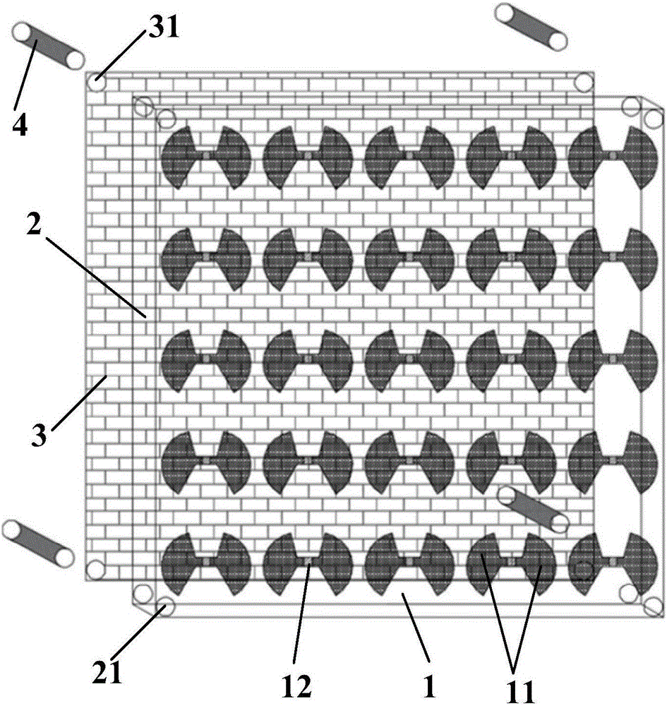
[0018] figure 1 It is an overall development schematic diagram of the present invention, including a loaded dipole antenna array 1, a dielectric substrate 2, a metal floor 3, and plastic screws 4 connecting the dipole antenna array and the metal floor. Described dipole antenna array is to be printed on the high loss FR4 (relative permittivity is 4.4, loss tangent is 0.02) dielectric substrate 2 that is printed on thickness 0.8mm Periodically arranged by many dipole units 11 Formed, the dipole unit 11 is made of copper sheets printed on the dielectric substrate 2 like butterfly wings, and the shape and size of each unit structure are exactly the same; the welding at both ends of the chip resistor 12 The points are respect...


PUM


Abstract

The invention discloses an ultra wideband wave absorber based on resistance loading. The ultra wideband wave absorber comprises a dipole array antenna, patch resistors, a metal floor and four plastic screws, wherein the four plastic screws are used for locating and fixing the dipole array antenna and the metal floor, the dipole array antenna is formed by periodically arranging a plurality of same dipoles similar to butterfly wings, two welding points of a single patch resistor are separately welded at the two ends of a dipole arm so as to further achieve perfect matching with a single dipole, and an electromagnetic wave can be absorbed by the dipole array antenna and is consumed by the patch resistors so as to achieve the purpose of wave absorption. The ultra wideband wave absorber can be applied to a microwave / millimeter-wave anti-interference system and has the advantages of simplicity in structure, light weight, low cost, unit miniaturization and short processing period; and moreover, the electromagnetic wave absorption within different frequency ranges can be achieved by designing dipole antennas in different frequency ranges.

Description

technical field [0001] The invention belongs to the technical field of microwave absorbing materials, and relates to an ultra-broadband absorber. Background technique [0002] With the rapid development of modern communication, more and more electromagnetic waves in space are becoming more and more complex, which will inevitably cause interference to other systems and make the system unable to work normally, and wave absorption also plays a vital role in the stealth of the antenna. It can reduce the radar cross-sectional area of ​​the antenna, which is exactly what the stealth antenna pursues. With the development of electronic countermeasures technology, higher requirements are put forward for the absorbing structure. The direction of the planarization of the absorbing structure is developing. Therefore, the ultra-broadband research of absorbing structures is still a hotspot in the industry and academia. [0003] In order to test the broadband characteristics of absorbing...

Claims


Application Information

Patent Timeline
IPC IPC(8): H01Q17/00
CPCH01Q17/00H01Q17/007
Inventor 林先其梅鹏张鹏程王伟陈哲刘士林庞平苏一洪
Owner UNIV OF ELECTRONIC SCI & TECH OF CHINA
Why Eureka
Try Eureka