Polarization plate, screen module group and manufacturing method of the screen module group

A polarizing plate and module technology, applied in optics, optical elements, polarizing elements, etc., can solve the problems of unprotected touch sensors, touch sensor damage, TP scrapping, etc., to facilitate visual inspection, reduce production costs, The effect of protection from damage

Inactive Publication Date: 2016-10-19
EVERDISPLAY OPTRONICS (SHANGHAI) CO LTD
View PDF5 Cites 6 Cited by
  • Summary
  • Abstract
  • Description
  • Claims
  • Application Information

AI Technical Summary

Problems solved by technology

[0004] However, since the thickness of the optical adhesive layer 12 (about 0.12-0.15 mm) is much greater than the thickness of the adhesive layer in the polarizer 12 (about 0.01-0.03 mm); therefore, when the screen module needs to be reworked, it will Choosing to peel off the optical adhesive layer 12 will easily cause damage to the touch sensor (Touch Sensor) on the touch screen 13, and even cause the entire touch screen 13 to be scrapped
[0005] In addition, the defect rate of the current TP full lamination technology is very high, that is, there are many reworked products, and because the OCA and the touch sensor on the TP will be in direct contact, the touch sensor will be unprotected when the bad rework is separated, which is extremely difficult. It is easy to cause TP to be scrapped, which greatly increases the cost of production

Method used


Image

  • Polarization plate, screen module group and manufacturing method of the screen module group
  • Polarization plate, screen module group and manufacturing method of the screen module group
  • Polarization plate, screen module group and manufacturing method of the screen module group

Examples


Embodiment 1

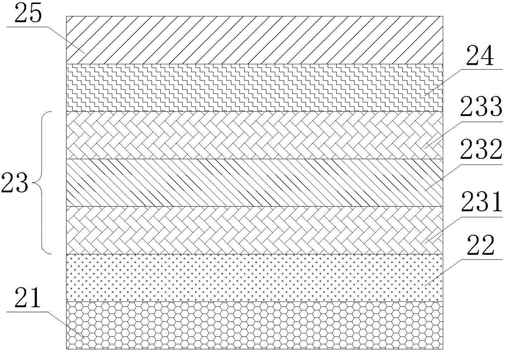
[0059] figure 2 It is a schematic structural diagram of a polarizing plate in the embodiment of the present application; as figure 2 As shown, a polarizing plate includes a release layer 21, a compensating film layer 22, a polarizing film 23, an adhesive layer 24 and a protective film 25; the above-mentioned polarizing film 23 has a light emitting front (ie figure 2 the top surface shown in ) and the back side for light incidence relative to that front side (i.e. figure 2 The lower surface shown), the above-mentioned compensation film layer 22 is covered on the lower surface of the polarizing film, and the release layer 21 is used as a base to cover the lower surface of the compensation film layer 22; meanwhile, the above-mentioned adhesive layer 24 and protective film 25 is stacked on the upper surface of the polarizing film 23 smoothly from bottom to top (that is, the above-mentioned compensation film layer 22, polarizing film 23, adhesive layer 24 and protective film 2...

Embodiment 2

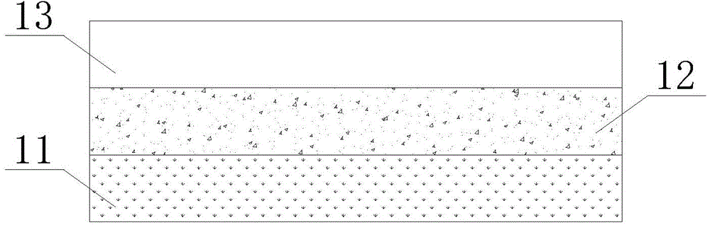
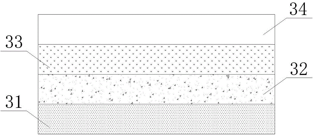
[0063] image 3 It is a schematic structural diagram of the screen module in the embodiment of the present invention; image 3 As shown, the present application also provides a screen module, including a panel (panel) 31, an optical adhesive layer (OCA) 32, a polarizer 33 and a touch panel (TP) 34; the above-mentioned panel 31 has a front surface for light emission , and the optical adhesive layer 32 covers the front surface of the panel 31 , the polarizer 33 covers the upper surface of the optical adhesive layer 32 , and the touch panel 34 is disposed on the upper surface of the polarizer 33 .

[0064] Further, the above-mentioned polarizing plate 33 can be the polarizing plate structure described in the first embodiment above (ie figure 1 ) The structure shown in 2), that is, the polarizer 33 may also include such as figure 1 The structures of the release layer 21, compensation film layer 22, polarizing film 23, adhesive layer 24 and protective film 25 shown in the illustr...

Embodiment 3

[0068] Figure 4 It is a schematic flow chart of a method for preparing a screen module in an embodiment of the present invention; as Figure 4 As shown, a method for preparing a screen module can be applied to prepare the screen module (such as an AMOLED display device, etc.) described in the second embodiment above, such as Figure 2-4 As shown, the method includes:

[0069] First, a panel 31 is provided, and the panel 31 has a front surface for emitting light.

[0070] Secondly, after assembling the IC module and the flexible circuit board FPC (not marked in the figure) on the front surface of the panel 31 , a module test (Module) is performed on the panel 31 .

[0071] Afterwards, the touch panel 34 attached with the polarizer 33 is attached to the panel 31 that has completed the above-mentioned module test and meets the process requirements through the optical adhesive layer 32, so as to form a new screen module.

[0072] Further, by providing a touch panel 34 with a f...


PUM

PropertyMeasurementUnit
Thicknessaaaaaaaaaa

Abstract

The polarizing plate, the screen module and the preparation method of the screen module provided by the present invention relate to the field of semiconductor device manufacturing, all of which can be based on the traditional structure of the screen module, by arranging the adhesive layer between the polarizing plate and the protective film Even if the polarizer is directly attached to the touch panel, it can not only minimize the pollution damage to the device structure during the manufacturing process, but also facilitate visual inspection, so that the contaminated device structure can be found in time to continue Subsequent rework operation; In addition, in the above-mentioned rework operation process, the thicker optical adhesive layer is generally separated, and since the polarizer is attached to the touch panel during the separation operation, It can effectively protect the touch sensor on the touch panel from damage, thereby effectively improving the efficiency of heavy industrial operations and greatly reducing production costs.

Description

technical field [0001] The invention relates to the field of semiconductor device manufacturing, in particular to a polarizing plate, a screen module and a method for preparing the screen module. Background technique [0002] At present, in the manufacturing process of display devices (such as AMOLED display devices, etc.), it is generally necessary to attach a polarizer on the cover glass of the panel (Panel) to form a screen module. [0003] figure 1 It is a schematic structural diagram of a traditional screen module; figure 1 As shown, a conventional display module generally includes a sandwich structure composed of a polarizer 11, an optical clear adhesive (OCA for short) 12 and a touch panel (TP for short) 13, and the optical clear adhesive 12 is disposed on Between the polarizer 11 and the touch screen 13 , that is, the optical adhesive layer 12 is directly attached to the surface of the touch screen 13 . [0004] However, since the thickness of the optical adhesive...

Claims


Application Information

Patent Timeline
IPC IPC(8): G02B5/30G02B1/14G06F3/041
Inventor 吴晓涛黄成沛
Owner EVERDISPLAY OPTRONICS (SHANGHAI) CO LTD
Why Eureka
Try Eureka