Array substrate, driving method and display device thereof

A technology of an array substrate and a driving method, which is applied to static indicators, instruments, etc., can solve problems affecting the display quality of liquid crystal display devices, TFT characteristic deviation, etc., and achieve the effects of improving display quality, reducing power consumption, and simplifying driving circuits

Active Publication Date: 2017-04-26
SHANGHAI TIANMA MICRO ELECTRONICS CO LTD +1
View PDF5 Cites 19 Cited by
  • Summary
  • Abstract
  • Description
  • Claims
  • Application Information

AI Technical Summary

Problems solved by technology

[0004] Although the low-frequency driving technology can significantly reduce power consumption, the thin-film transistor remains in the constant-level maintenance stage for a long time during the suspension period, which will cause TFT characteristic deviation and affect the display quality of the liquid crystal display device.

Method used


Image

  • Array substrate, driving method and display device thereof
  • Array substrate, driving method and display device thereof
  • Array substrate, driving method and display device thereof

Examples


Embodiment Construction

[0043] Embodiments of the present invention provide an array substrate, a driving method thereof, and a display device. The embodiments of the present invention will be described in detail below with reference to the accompanying drawings.

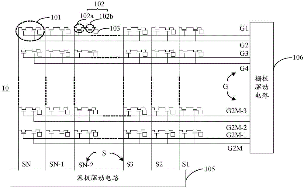
[0044] refer to figure 1 , figure 1 It is a schematic structural diagram of an array substrate according to an embodiment of the present invention. The array substrate 10 includes: a plurality of scanning lines G, a plurality of data lines S, and the intersection of the plurality of scanning lines G and the plurality of data lines S defines a A plurality of pixel units 101 , a source driving circuit 105 and a gate driving circuit 106 are arranged in an array. Wherein, each pixel unit 101 includes a plurality of series-connected thin film transistors 102 and a pixel electrode 103, the gate of each thin-film transistor in the plurality of series-connected thin film transistors 102 is respectively electrically connected to a different scanni...


PUM


Abstract

The invention relates to an array substrate, a driving method and a display device thereof. The array substrate comprises a plurality of scanning lines, a plurality of data lines, a source electrode driving circuit and a gate driving circuit, wherein a plurality of pixel units are defined by the crossing of the scanning lines and data lines; each of the pixel units comprises a plurality of serially connected thin film transistors and a pixel electrode; the grid electrodes of the serially connected thin film transistors are respectively in electric connection with different scanning lines; all the pixel electrodes are electrically connected with the data lines through the serially connected thin film transistors; a time interval for writing two adjacent data voltage signals into the pixel units includes a first time period and a second time period; in the first time period, the data voltage signal inputted by the source electrode driving circuit is written into the pixel electrodes; in the second time period, each thin film transistor is at least opened for one time and the plurality of serially connected thin film transistors cannot be simultaneously under opening state. The array substrate according to the embodiment of the invention can reduce the power consumption and can reduce the TFT characteristic drifting.

Description

technical field [0001] The present invention relates to the field of display technology, in particular to an array substrate, a driving method thereof, and a display device. Background technique [0002] In recent years, liquid crystal display devices have been widely used in information terminals such as computers, smart phones, mobile phones, car navigation devices, and e-books. There are many types of liquid crystal displays, among which thin film transistor (Thin Film Transistor, TFT) liquid crystal displays are used because of their applicable temperature With the advantages of wide range, high degree of automation in manufacturing technology, easy integration, and good environmental protection characteristics, it is gradually becoming a mainstream display product. How to reduce the power consumption of thin film transistor liquid crystal display devices and improve the quality of display images has become a current research hotspot. [0003] With the development of li...

Claims


Application Information

Patent Timeline
Patent Type & Authority Applications(China)
IPC IPC(8): G09G3/36
CPCG09G3/3648G09G2310/0202
Inventor 席克瑞许祖钊林柏全李金玉
Owner SHANGHAI TIANMA MICRO ELECTRONICS CO LTD
Why Eureka
Try Eureka