Display panel and manufacturing method thereof

A technology for display panels and display substrates, used in semiconductor/solid-state device manufacturing, organic semiconductor devices, electrical components, etc., can solve the problems of pressure damage OLED, OLED bombardment, affecting device performance and lifespan, etc., to reduce damage and simplify the process. , the effect of reducing the complexity of the process

Active Publication Date: 2017-06-13
BOE TECH GRP CO LTD
View PDF6 Cites 17 Cited by
  • Summary
  • Abstract
  • Description
  • Claims
  • Application Information

AI Technical Summary

Problems solved by technology

However, for OLED displays, the intrusion of water and oxygen seriously affects the performance and lifetime of the device
In the prior art, in order to enhance the packaging effect, water-absorbing materials are usually added to the packaging material coated in the gap between the cover plate and the display substrate, but the water-absorbing materials often cause damage to the device, because one: when the water-absorbing particles react with water, they will Release traces of gas or heat, such as CaO releases heat, and the OLED directly in contact with it will be bombarded, resulting in dark spots; 2. The surface of the water-absorbing particles is rough and evenly distributed in the coated packaging material. When the volume of the packaging material changes, Particles close to OLED will crush OLED under external pressure
Therefore, it is usually completed by means of batch coating. For example, in an existing two-layer coating scheme, when coating an encapsulation material on an OLED substrate, the first layer is printed by inkjet printing (Ink JetPrinting, IJP ) coating common materials, curing, the second layer coating water-absorbing material, and then press-fit packaging, so that although the water-absorbing material is kept away from the OLED, the damage to the OLED is reduced, but the two coatings increase the process complexity Spend

Method used


Image

  • Display panel and manufacturing method thereof
  • Display panel and manufacturing method thereof
  • Display panel and manufacturing method thereof

Examples


Embodiment Construction

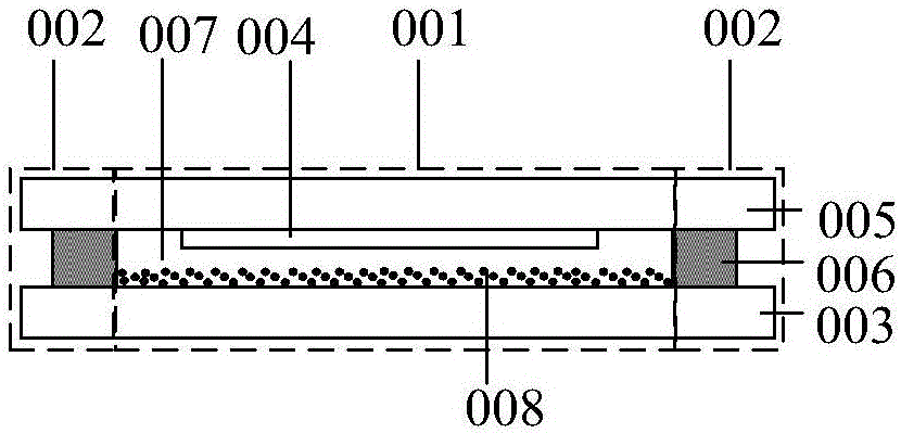
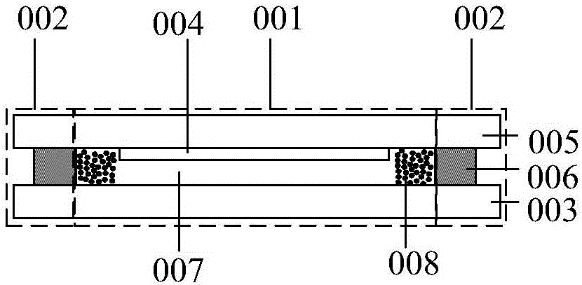
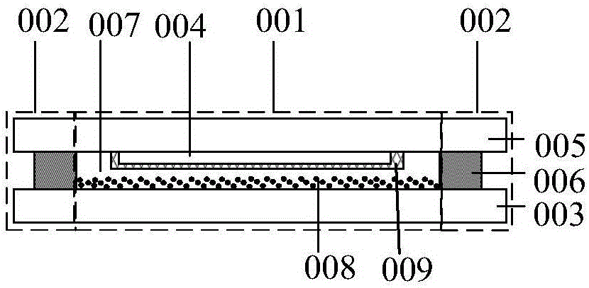
[0039] In order to solve the above technical problems, embodiments of the present invention provide a display panel and a manufacturing method thereof. Among them, the display panel provided by the embodiment of the present invention has a display area and a frame sealant area surrounding the display area. The display panel includes a cover plate, a display substrate with an OLED device, and a frame sealant area located between the display substrate and the cover plate. The sealant and the encapsulation layer located in the display area between the display substrate and the cover plate; wherein the OLED device is located in the display area; the vertical film layer inside the encapsulation layer is distributed on the side away from the OLED device with water-absorbing magnetic properties Nano particles, or magnetic nanoparticles with water absorption are distributed along the film layer direction inside the encapsulation layer around the area where the OLED device is located.

[...


PUM


Abstract

The embodiment of the invention discloses a display panel and a manufacturing method thereof. According to the scheme, on one hand, magnetic nanoparticles with water absorption are distributed on the side, away from an OLED device, in the perpendicular film direction in a packaging layer or on the periphery of the area where the OLED device is located in the film direction; on the other hand, due to the fact that the magnetic nanoparticles with the water absorption have magnetism, in the packaging waterproofing technology, the magnetic nanoparticles with the water absorption can be doped in packaging materials, the magnetism is applied to induce the magnetic nanoparticles to the side away from an OLED device or the periphery of the area where the OLED device is located, and therefore a person only needs to conduct one-time coating on the packaging materials doped with the magnetic nanoparticles with the water absorption; compared with the double coating mode in the prior art, the technology is simple, and the technology complexity is lowered.

Description

Technical field [0001] The present invention relates to the field of display technology, in particular to a display panel and a manufacturing method thereof. Background technique [0002] Organic Light-emitting Diode (OLED) as a new display technology has attracted more and more attention. However, for OLED displays, the intrusion of water and oxygen seriously affects the performance and life of the device. In the prior art, in order to enhance the packaging effect, a water-absorbing material is usually added to the packaging material coated in the gap between the cover plate and the display substrate. However, the water-absorbing material often causes damage to the device, because one: the water-absorbing particles will react with water. Release trace amounts of gas or heat. For example, CaO releases heat, and the OLED directly in contact with it will be bombarded, resulting in dark spots; 2. The surface of the water-absorbing particles is rough and evenly distributed in the co...

Claims


Application Information

Patent Timeline
Patent Type & Authority Applications(China)
IPC IPC(8): H01L51/52H01L51/56
CPCH10K50/841H10K50/846H10K71/00H10K59/00H10K2102/331H10K50/8426
Inventor 于东慧
Owner BOE TECH GRP CO LTD
Why Eureka
Try Eureka