Display panel and manufacturing method thereof

A display panel and substrate technology, applied in nonlinear optics, instruments, optics, etc., can solve the problems of low mass production efficiency, low liquid crystal margin of display panel, small step difference, etc., to improve liquid crystal margin and improve mass production. rate effect

Inactive Publication Date: 2018-01-16
HKC CORP LTD
View PDF9 Cites 8 Cited by
  • Summary
  • Abstract
  • Description
  • Claims
  • Application Information

AI Technical Summary

Problems solved by technology

However, when this design is applied to a liquid crystal display panel, the step difference between the main spacer and the auxiliary spacer will be too small, resulting in a relatively low and too small liquid crystal margin (LC margin) of the liquid crystal display panel, and relatively low mass production efficiency. lower

Method used


Image

  • Display panel and manufacturing method thereof
  • Display panel and manufacturing method thereof
  • Display panel and manufacturing method thereof

Examples


Embodiment Construction

[0028] The description of the following embodiments refers to the attached drawings to illustrate specific embodiments that can be implemented in this application. The direction terms mentioned in this application, such as "up", "down", "front", "rear", "left", "right", "inner", "outer", "side", etc., are for reference only The direction of the additional schema. Therefore, the directional terms used are used to illustrate and understand the application, rather than to limit the application.

[0029] The drawings and descriptions are to be regarded as illustrative in nature and not restrictive. In the figures, units with similar structures are indicated by the same reference numerals. In addition, for understanding and ease of description, the size and thickness of each component shown in the drawings are arbitrarily shown, but the application is not limited thereto.

[0030] In the drawings, the thickness of layers, films, panels, regions, etc., are exaggerated for clarity. In...


PUM


Abstract

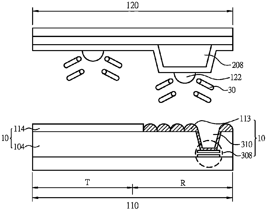
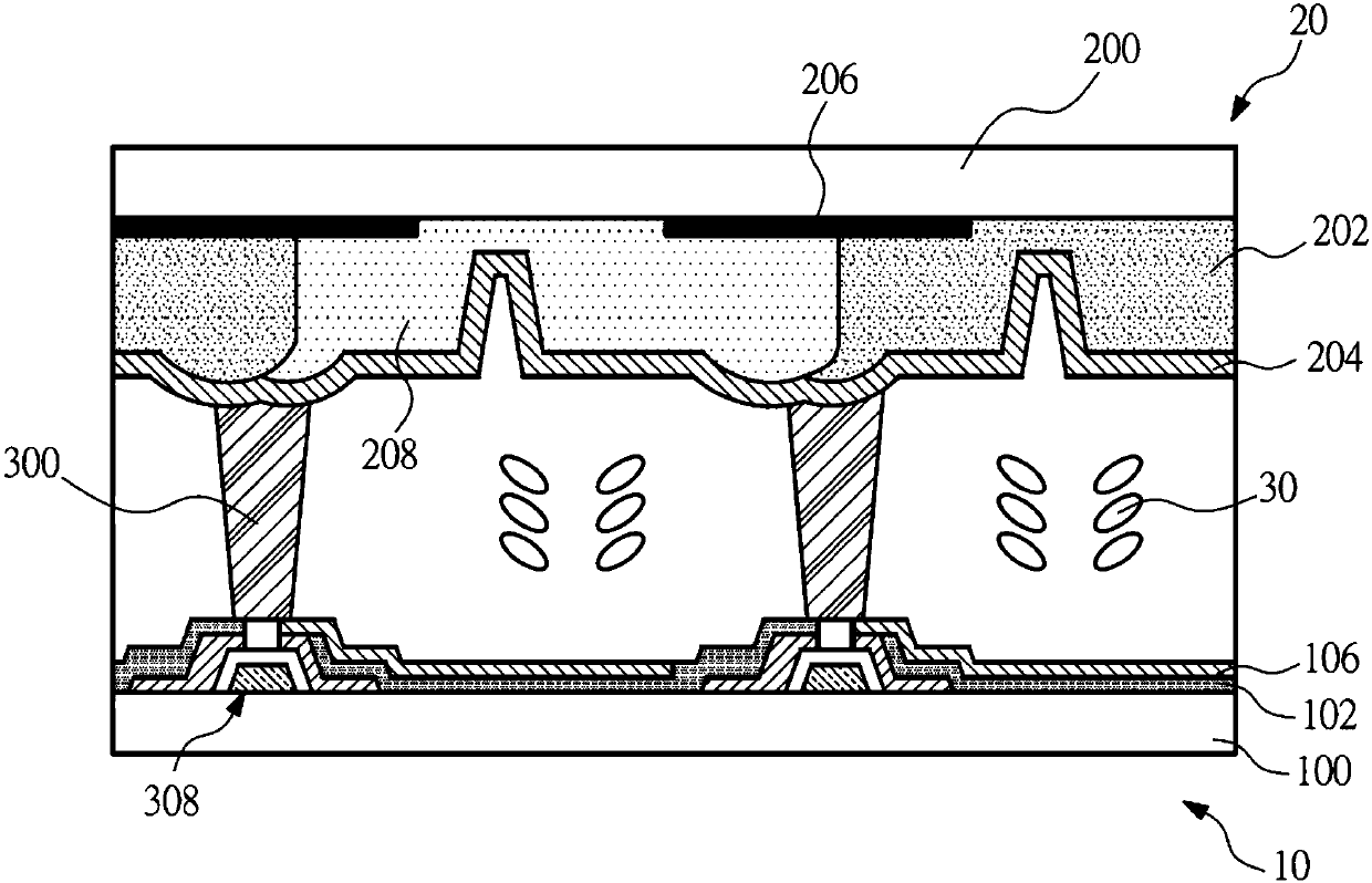
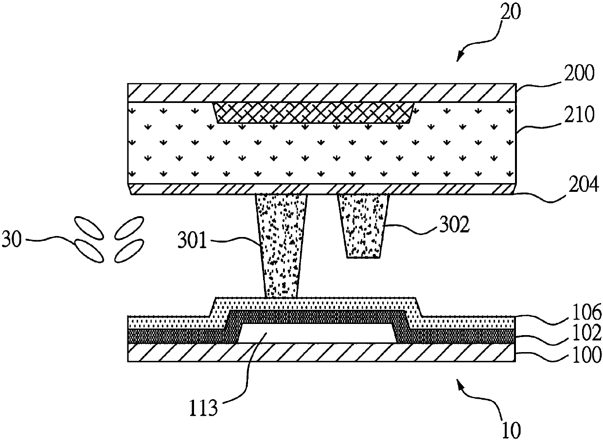
The invention discloses a display panel and a manufacturing method thereof. The display panel comprises a first substrate and a second substrate which are opposite, a color filter layer which is formed between the first substrate and the second substrate, a first part and a second part which have different heights, two electrode layers which are formed on the opposite surfaces of the first substrate and the second substrate respectively, and light partition objects which include the first partition object opposite to the first part in position and the second partition object opposite to the second part in position. The total height of the first partition object and the second part is larger than that of the second partition object and the second part. By increasing the segment gap of the main partition object and the auxiliary partition object of the display panel, the situation that the self deviation situation of the substrate can not restore when the partition objects are interferedwith by overlapping parts can be reduced, and the liquid crystal margin of the liquid crystal display panel can be improved when the display panel is used for the liquid crystal display panel.

Description

Technical field [0001] This application relates to a manufacturing method, in particular to a display panel and a manufacturing method thereof. Background technique [0002] With the advancement of science and technology, displays with many advantages such as power saving, no radiation, small size, low power consumption, flat plane, high resolution, stable picture quality, etc., especially today's various information products such as: mobile phones, notebooks The increasing popularity of computers, digital cameras, PDAs, screens and other products has also greatly increased the demand for display panels. Therefore, how to improve the production process efficiency and product yield will be a problem that operators must face. [0003] The display panel includes two oppositely arranged substrates, which can be an active switch array substrate and a color filter substrate, or a combination of an array substrate combined with a color filter and an opposite substrate. In order to ensur...

Claims


Application Information

Patent Timeline
Patent Type & Authority Applications(China)
IPC IPC(8): G02F1/1339G02F1/1335G02F1/13
CPCG02F1/13396G02F1/136209G02F1/1368G02F1/136222
Inventor 黄北洲
Owner HKC CORP LTD
Why Eureka
Try Eureka