Image sensor and method of forming the same

An image sensor and optical filter technology, which is applied in semiconductor devices, electric solid devices, radiation control devices, etc., to achieve the effects of avoiding crosstalk and making full use of the light-transmitting area

CN108336103BActive Publication Date: 2020-12-18淮安西德工业设计有限公司
6 Cites 0 Cited by

Patent Information

Authority / Receiving Office
CN · China
Patent Type
Patents(China)
Current Assignee / Owner
Publication Date
2020-12-18

Smart Images

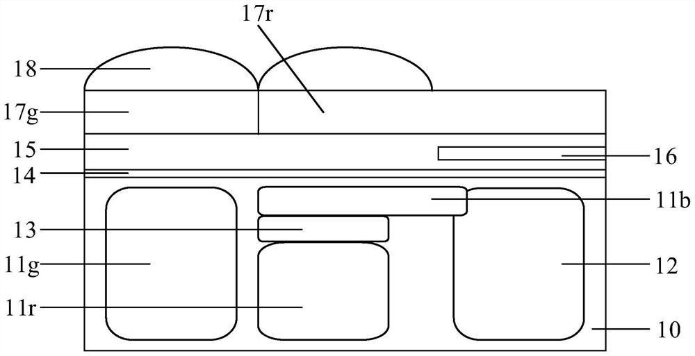
  • Figure 1
    Figure 1
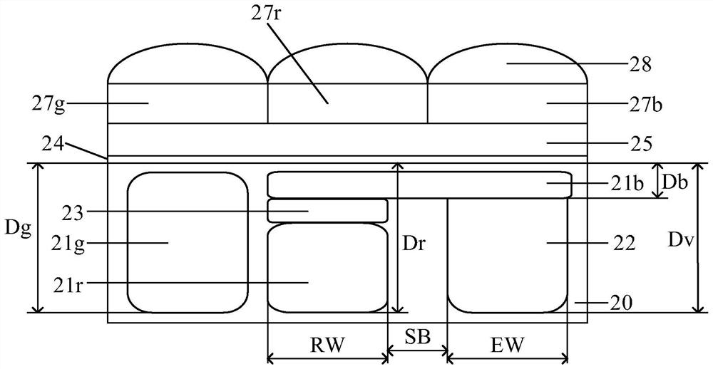
  • Figure 2
    Figure 2
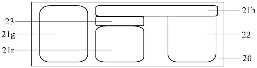
  • Figure 3
    Figure 3
Patent Text Reader

Abstract

The invention discloses an image sensor and a forming method thereof. The image sensor comprises a semiconductor substrate; a photodiode for absorbing green light, a photodiode for absorbing blue light, a photodiode for absorbing red light and a vertical charge transfer layer which are arranged in the semiconductor substrate; the photodiode for absorbing the green light, the photodiode for absorbing the red light and the vertical charge transfer layer are spaced apart from each other, and the photodiode for absorbing the blue light is arranged on the photodiode for absorbing the red light andextends to cover the vertical charge transfer layer; the image sensor further comprises a planarization layer arranged on the semiconductor substrate, and a filter layer and a micro lens arranged on the planarization layer, the filter layer includes a green filter, a magenta filter and a blue filter, the photodiode for absorbing the green light corresponds to the lower portion of the green filter,the photodiode for absorbing the red light corresponds to the lower portion of the magenta filter, and the vertical charge transfer layer corresponds to the lower portion of the blue filter. According to the image sensor, crosstalk of light to the vertical charge transfer layer is avoided, and the light transmissive area of the image sensor is increased.
Need to check novelty before this filing date? Find Prior Art

Description

technical field

[0001] The invention belongs to the technical field of image sensor manufacturing technology, and in particular relates to an image sensor and a forming method thereof. Background technique

[0002] In general, an image sensor is a semiconductor device used to convert an optical image into an electrical signal. Image sensors are classified into charge-coupled device (Charge-Coupled Device, CCD) and complementary metal oxide semiconductor (Complementary Metal Oxide Semiconductor, CMOS) image sensors.

[0003] Traditional image sensors use red, green and blue color filters, and there are photodiodes under the corresponding filters that absorb light of the corresponding wavelength. The vertical pixel structure utilizes the correlation between the absorption depth of visible light incident on the semiconductor material and the wavelength, that is, the absorption depth of short-wavelength light is small, and the absorption depth of long-wavelength light is large,...

Examples

Embodiment Construction

[0036] In the prior art, since a metal barrier layer is added on the vertical charge transfer layer to reflect the light above the vertical charge transfer layer, the crosstalk of light to the vertical charge transfer layer is reduced, but the existence of the metal barrier layer makes the above The light-transmitting area is wasted, and the filling rate of the image sensor is reduced, thereby reducing the performance of the image sensor.

[0037] In response to the above problems, the technical solution of the present invention provides a new type of image sensor based on a vertical pixel structure, which expands the area of ​​the photodiode that absorbs blue light to cover the vertical charge transfer layer, thus avoiding the crosstalk of light to the vertical charge transfer layer, At the same time, the metal light-blocking structure on the vertical charge transfer layer is removed to increase the light-transmitting area, so as to realize a high-performance image sensor.

...