
Method for measuring light intensity distribution
A light intensity distribution and measurement method technology, applied in the field of light intensity distribution measurement, can solve the problems of low sensitivity of thermal sensors, narrow light wave band, and low resolution, and achieve high sensitivity, high absorption rate, high resolution and accuracy degree of effect
- Summary
- Abstract
- Description
- Claims
- Application Information
AI Technical Summary
Problems solved by technology
Method used
Image

Examples
Embodiment Construction
[0031] The method for detecting light intensity distribution provided by the present invention will be further described in detail below in conjunction with the accompanying drawings and specific embodiments.
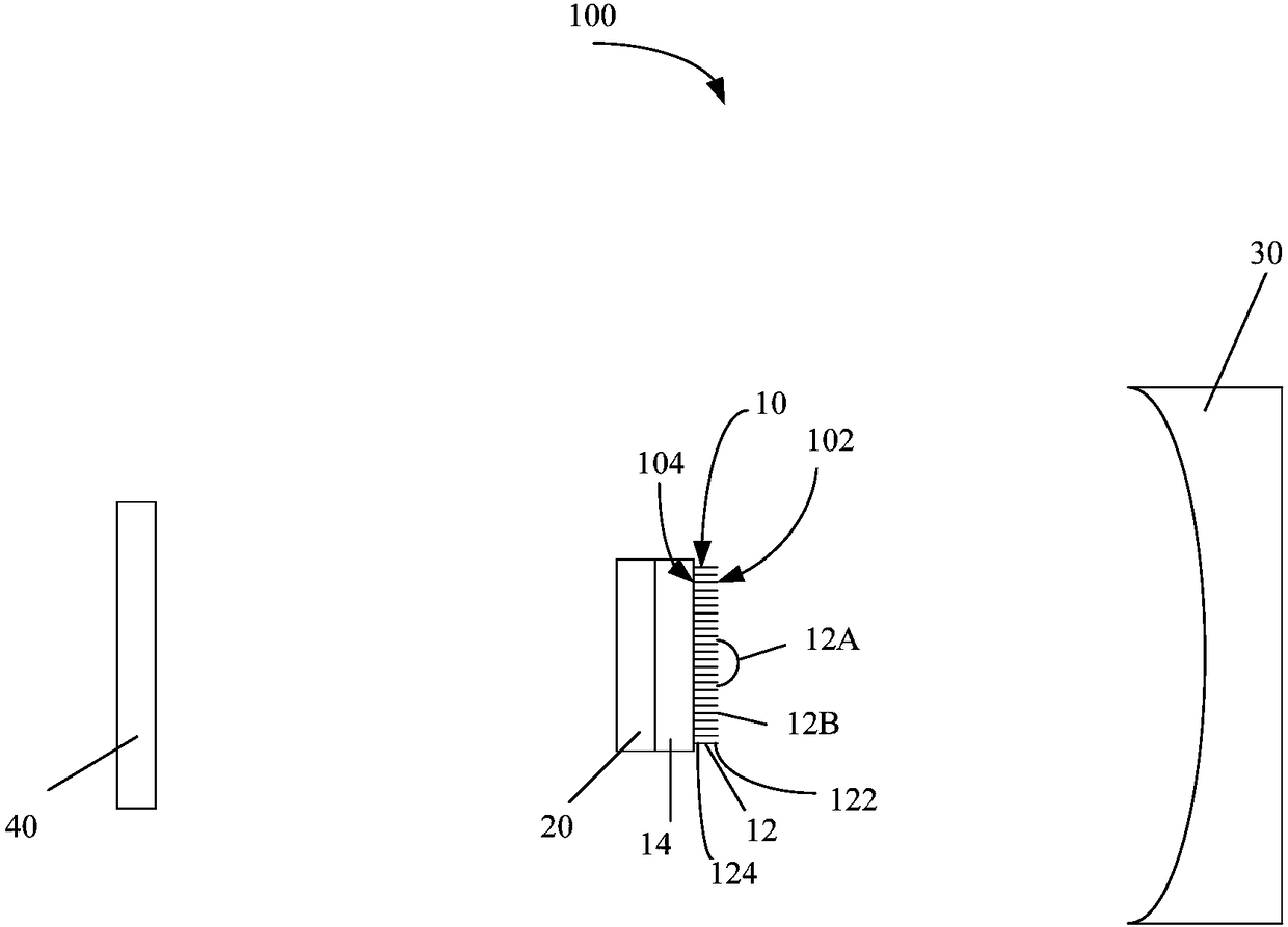
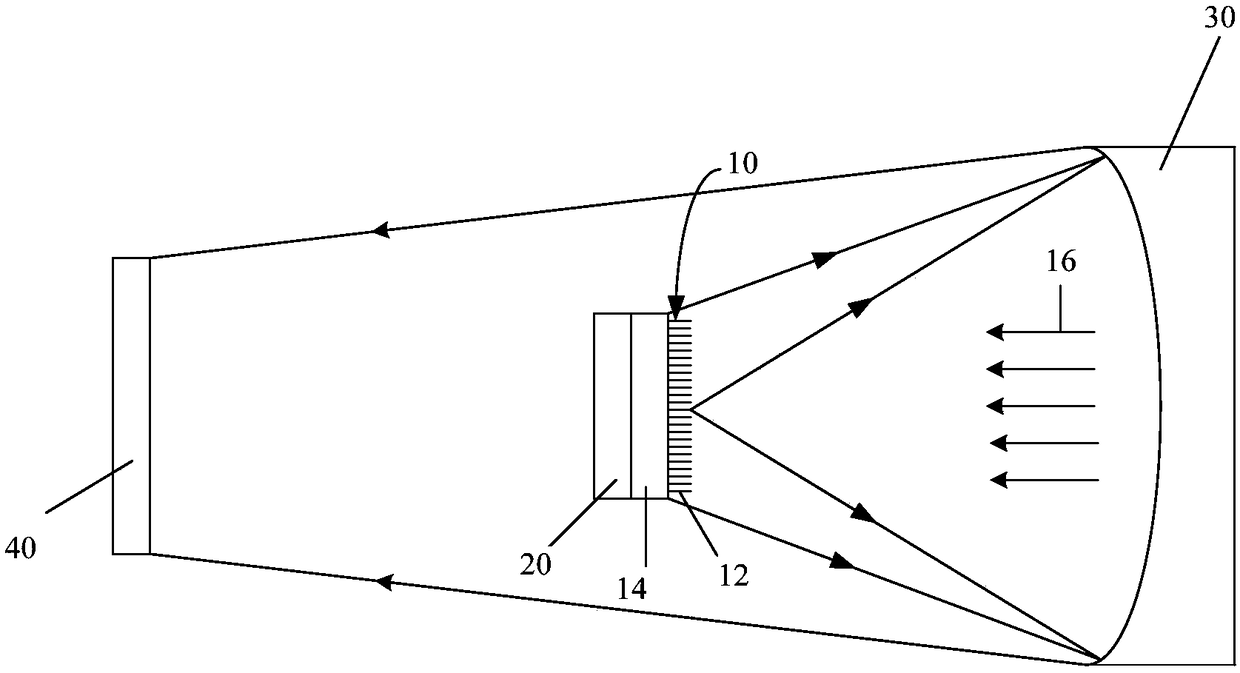
[0032] See figure 1 , the embodiment of the present invention provides a detection system 100 of light intensity distribution, comprising: a carbon nanotube array 10 disposed on the surface of a growth substrate, a cooling device 20 , a mirror 30 and an imaging element 40 . The cooling device 20 is arranged between the imaging element 40 and the growth substrate 14, and the cooling device is used to cool the growth substrate 14 so that the contact surface between the growth substrate 14 and the carbon nanotube array 10 maintains a constant temperature; The mirror 30 is spaced from the carbon nanotube array 10 , and the carbon nanotube array 10 is disposed between the mirror 30 and the growth substrate 14 ; the imaging element 40 is spaced from the cooling device 20 .
...
PUM
 Abstract
Description
Claims
Application Information