A kind of super barrier diode device

A technology of super-barrier diodes and devices, applied in semiconductor devices, electrical components, circuits, etc., can solve the problems of poor reverse blocking ability and low forward current density, so as to improve rectification efficiency and voltage blocking. ability, the effect of increasing the forward current level

Active Publication Date: 2021-09-24
UNIV OF ELECTRONICS SCI & TECH OF CHINA
View PDF4 Cites 0 Cited by
  • Summary
  • Abstract
  • Description
  • Claims
  • Application Information

AI Technical Summary

Problems solved by technology

[0006] Aiming at the problems of low forward conduction current density and poor reverse blocking ability of the above-mentioned traditional super-barrier diode, the present invention proposes a super-barrier diode device, which can increase the forward conduction current density and improve the voltage blocking ability , the forward conduction current level of the device is significantly improved by setting the trench structure; the multi-subcurrent branch in the conduction state of the device is increased by adding a heterojunction, and the forward conduction current level of the device is improved again; in addition, a superjunction The structure is used to improve the voltage blocking capability of the device while reducing the forward conduction resistance of the device, and obtain a good compromise between reverse blocking and forward voltage drop

Method used


Image

  • A kind of super barrier diode device
  • A kind of super barrier diode device
  • A kind of super barrier diode device

Examples


Embodiment 1

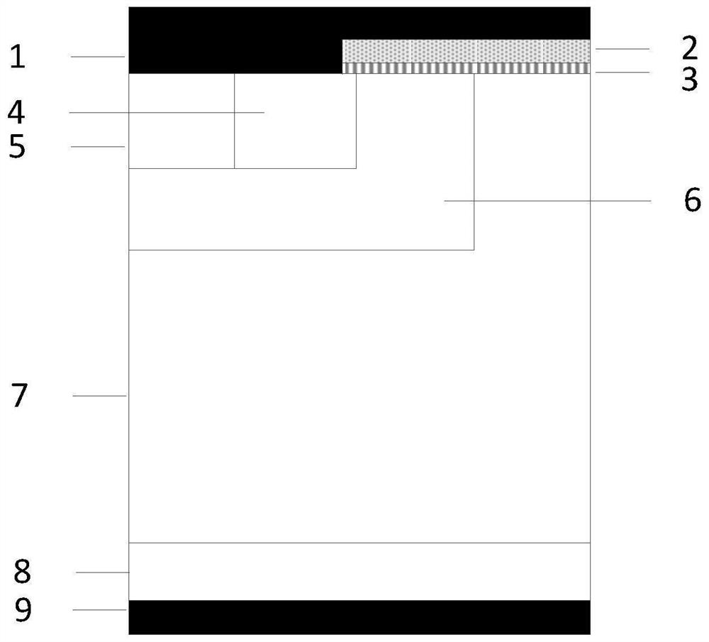
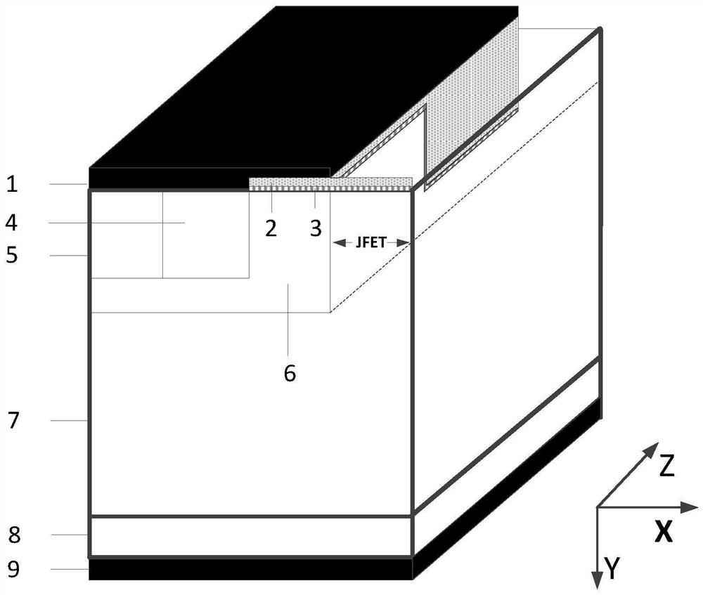
[0071] In this embodiment, the structure of a 1200V super-barrier diode device is taken as an example. The body material is silicon carbide, and the schematic diagram of its cell is as follows figure 2 shown. Including cathode metal 9, N+ silicon carbide substrate 8 and N- silicon carbide drift region 7 arranged in sequence from bottom to top, a P-type silicon carbide base region 6 is set on the left side of the top layer of the N- silicon carbide drift region 7, and a P-type silicon carbide The left side of the top layer of the base region 6 is arranged side by side from left to right in close contact with the P+ silicon carbide contact region 5 and the N+ silicon carbide source region 4, and the depth of the N+ silicon carbide source region 4 does not exceed the depth of the P+ silicon carbide contact region 5; The upper surface of the right side of the silicon carbide source region 4, the upper surface of the P-type silicon carbide base region 6 on the right side of the N+...

Embodiment 2

[0074] This embodiment makes a certain degree of modification to embodiment 1, and its structure is roughly the same as embodiment 1, the difference is that there is also an anode metal 1 inside the groove structure, that is, the depth of the bottom of the anode metal 1 is deeper than that of the groove at the top of the structure, such as Figure 8 shown. This improvement can reduce the gate resistance, increase the charging speed of the gate charge, and further optimize the rectification performance of the device, so that the gate control capability of the device is further improved.

Embodiment 3

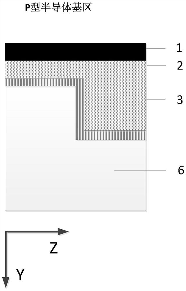
[0076] This embodiment makes some modifications to Embodiment 1 and Embodiment 2, and its structure is roughly the same as that of Embodiment 2, the difference is that the N-SiC drift region 7 on the right side of the P-type SiC The right side of the surface does not have a layer of dielectric layer 3, the dielectric layer 3 is replaced by polysilicon 2, polysilicon 2 and N-silicon carbide drift region 7 form a Si / SiC heterojunction, the junction width is about 0.1 μm ~ 0.4 μm ,Such as Figure 9 shown. The super-barrier diode in this embodiment has a three-dimensional super-barrier structure and a Si / SiC heterojunction, which increases the number of sub-current branches in the on-state of the device, and improves the performance of the diode in this embodiment again. Forward conduction current level.


PUM

PropertyMeasurementUnit
thicknessaaaaaaaaaa
widthaaaaaaaaaa
thicknessaaaaaaaaaa

Abstract

A super-barrier diode device belongs to the technology in the field of semiconductor power devices. Its cellular structure includes a cathode metal, an N+ semiconductor substrate, and an N-semiconductor drift region arranged sequentially from bottom to top. A P-type semiconductor base region is set on the left side of the top layer of the N-semiconductor drift region, and a P-type semiconductor base region is set on the left side of the top layer of the P-type semiconductor base region. The P+ semiconductor contact region and the N+ semiconductor source region in close contact are arranged side by side in order from left to right; the upper surface on the right side of the N+ semiconductor source region, the upper surface of the P-type semiconductor base region on the right side of the N+ semiconductor source region, and the P-type semiconductor base region A trench structure is set on the upper surface of the N-semiconductor drift region on the right; a gate structure is set on the trench structure, and the gate structure includes a dielectric layer, polysilicon and anode metal set from bottom to top, and the bottom surface of the polysilicon is lower on the top of the trench structure; the anode metal is arranged on the upper surface of the super barrier diode device. The invention improves the forward conduction current level and voltage blocking ability of the device.

Description

technical field [0001] The invention belongs to the technical field of power semiconductor devices, and in particular relates to a super barrier diode device structure. Background technique [0002] The anthropocene has entered the 21st century. Although various forms of new energy sources have emerged, such as wind energy, nuclear energy, solar energy, and geothermal energy, the world's energy production and consumption are still dominated by fossil energy, and fossil energy will remain in the long run. For a period of time, it occupies the most important seat of many energy needs of human beings. The large and long-term use of fossil energy will inevitably lead to a series of problems, which are closely related to the deterioration of global environmental problems such as global warming. A considerable proportion of fossil energy is converted into electricity. Electric energy is one of the main forms of energy that can be directly used by human beings, and the improvemen...

Claims


Application Information

Patent Timeline
Patent Type & Authority Patents(China)
IPC IPC(8): H01L29/861H01L29/06
CPCH01L29/0634H01L29/861
Inventor 张金平邹华王康罗君轶刘竞秀李泽宏张波
Owner UNIV OF ELECTRONICS SCI & TECH OF CHINA
Why Eureka
Try Eureka