A Photonic Crystal Waveguide Diagonal Mode Interference Fano Resonant Structure

A photonic crystal waveguide and resonant structure technology, applied in optical waveguides, light guides, optics, etc., can solve the problems of photonic crystal Fano resonance complex asymmetric structure, and achieve the effect of simple and symmetrical structure and reduced volume.

CN109669242BInactive Publication Date: 2021-01-01SHENZHEN UNIV
11 Cites 0 Cited by

Patent Information

Authority / Receiving Office
CN · China
Patent Type
Patents(China)
Current Assignee / Owner
Publication Date
2021-01-01
Estimated Expiration
Not applicable · inactive patent

Smart Images

  • Figure 1
    Figure 1
  • Figure 2
    Figure 2
  • Figure 3
    Figure 3
Patent Text Reader

Abstract

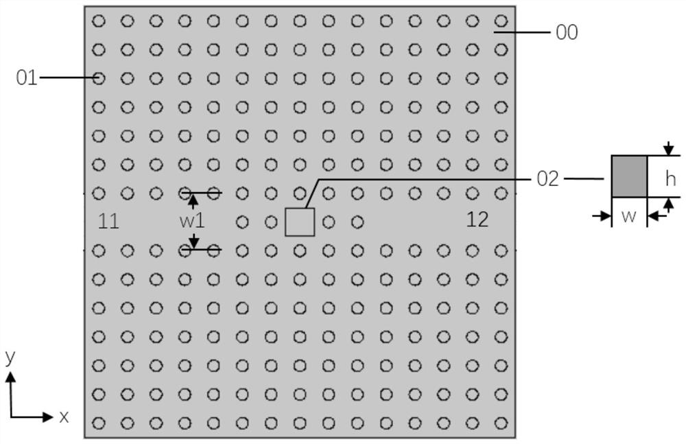
The invention discloses a photonic crystal waveguide diagonal mode interference FANO resonant structure. The structure comprises a two-dimensional photonic crystal linetype waveguide formed through distribution of a plurality of dielectric cylinders with the refractive index, the two-dimensional photonic crystal linetype waveguide comprises two waveguide ports and one point defect resonant cavity,wherein the two waveguide ports are arranged on the two sides of the point defect resonant cavity, the point defect resonant cavity comprises four dielectric cylinders and one point defect dielectriccylinder with one cross section being square or similar to square, two dielectric cylinders are symmetrically arranged on the two sides of the point defect dielectric cylinder respectively, and the centers of the four dielectric cylinders and the point defect dielectric cylinder are distributed and arranged at equal intervals. The structure provided by the invention is compact, bright mode and dark mode of Fano resonance can be conveniently controlled, and Fano resonance is easy to achieve integration with other photonic crystal parts.
Need to check novelty before this filing date? Find Prior Art

Description

technical field

[0001] The invention relates to the fields of photonic crystal point defect mode distribution and Fano resonance, in particular to a Fano resonance structure caused by interference of photonic crystal waveguide diagonal modes. Background technique

[0002] In recent years, photonic crystals have always been a hot field for people to study optical devices. Photonic crystals are crystal structures composed of materials with different dielectric constants arranged in periodic lattices. When the electromagnetic wave propagates in the photonic crystal, the Bragg scattering causes the electromagnetic wave to be modulated to form an energy band structure, and the electromagnetic wave in the forbidden band cannot propagate at all. The introduction of defects into photonic crystals can realize the guidance and control of electromagnetic waves, and thus various devices with different functions can be obtained, such as photonic crystal lasers, filters, sensors, etc. ...

Examples

Embodiment Construction

[0027] Below, the invention will be further described in conjunction with the accompanying drawings and specific implementation methods. It should be noted that, on the premise of no conflict, the various embodiments described below or the technical features can be combined arbitrarily to form a new embodiment. .

[0028] The following description serves to disclose the present invention to enable those skilled in the art to carry out the present invention. The preferred embodiments described below are only examples, and those skilled in the art can devise other obvious variations. The basic principles of the present invention defined in the following description can be applied to other embodiments, variations, improvements, equivalents and other technical solutions without departing from the spirit and scope of the present invention.

[0029] Those skilled in the art should understand that in the disclosure of the present invention, the terms "vertical", "transverse", "upper...