A semiconductor wafer cleaning device

A cleaning device and semiconductor technology, which is applied in semiconductor/solid-state device manufacturing, liquid cleaning methods, cleaning methods and utensils, etc., which can solve poor cleaning effects, inability to fix wafers, and inability to clean wafers from multiple angles, etc. question

Active Publication Date: 2020-10-20
JIANGSU NEPES SEMICON
View PDF4 Cites 1 Cited by
  • Summary
  • Abstract
  • Description
  • Claims
  • Application Information

AI Technical Summary

Problems solved by technology

[0003] Chinese patent (authorized announcement number: CN207503923U) discloses a semiconductor wafer cleaning device, including a conveyor belt, a liquid container is installed at the right end of the conveyor belt, a filter screen is installed in the middle of the liquid container, and a fixed frame, and a nozzle is installed in the middle of the fixed frame, the water pump and the nozzle are connected together through a high-pressure hose, and a light source is provided at both ends of the fixed frame, and a light source sensor is installed on the nozzle, but the above device does not The wafer cannot be cleaned from multiple angles, the cleaning effect is not good, and the device cannot effectively fix the wafer, and the wafer has the risk of falling. Therefore, in view of the above current situation, it is urgent to develop a semiconductor wafer cleaning device. In order to overcome the deficiencies in the current practical application

Method used


Image

  • A semiconductor wafer cleaning device
  • A semiconductor wafer cleaning device
  • A semiconductor wafer cleaning device

Examples


Embodiment 1

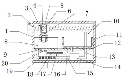
[0024] See Figure 1~3 In the embodiment of the present invention, a semiconductor wafer cleaning device includes a frame 1, a clamp 4, a water tank 8 and a spray device 10. The left side of the frame 1 is provided with a motor 2 which is bolted to the frame 1 , The motor 2 is provided with a screw rod connected to the frame 1 bearing on the lower side, the left side output end of the motor 2 is connected with a second gear, the left end of the screw rod is provided with a third gear, the second gear and the first gear Three gears are meshed and connected, a first fixing block 3 is provided on the screw rod, the first fixing block 3 is threadedly connected with the screw rod, a clamp 4 is provided on the front side of the first fixing block 3, and the screw rod is lower The side is provided with a fixed plate 12, the fixed plate 12 is fixedly connected to the frame 1, a water tank 8 is provided on the left side of the top of the fixed plate 12, and the water tank 8 is bolted to...

Embodiment 2

[0030] A cleaning equipment includes the semiconductor wafer cleaning device described in Embodiment 1.

[0031] In the semiconductor wafer cleaning device, the impurities in the water in the recovery box 17 are isolated from the bottom of the recovery box 17 through the first filter layer 18. The purified water passes through the water inlet pipe 9 and returns to the water tank 8, which avoids any damage to the water in the water tank 8. The water produces secondary pollution. By installing the second filter layer 19, the fine impurities in the water can be absorbed, which can purify the water quality, so that the water in the water tank 8 has a longer use time and saves water resources. With the movable frame 5, the clamp 4 can be moved up and down repeatedly, which is beneficial to enhance the cleaning degree of the wafer. By setting the electric guide roller 22, the wafer can be rotated and the wafer can be cleaned comprehensively, which is beneficial to enhance the cleaning e...


PUM


Abstract

The invention relates to the technical field of a semiconductor wafer technology and in particular relates to a semiconductor wafer washing device. The semiconductor wafer washing device comprises a framework, a clamp, a water tank and a spraying device, wherein a motor is arranged at the left side of the framework; a screw rod which is connected with the framework through a bearing is arranged atthe lower side of the motor; a first fixed block is arranged on the screw rod; the clamp is arranged at the front side of the first fixed block; a fixed plate is arranged at the lower side of the screw rod; the water tank is arranged at the left side of the top of the fixed plate; the spraying device is arranged at the right side of the water tank. According to the semiconductor wafer washing device, a gear and a movable frame are arranged so that up-down reciprocating motion of the clamp can be realized and the washing degree of a wafer is facilitated; an electric guide roller is arranged sothat the wafer can be rotated and the washing effect is facilitated; the spraying device is arranged so that the wafer can be sprayed and washed and the cleanliness of the wafer is improved; meanwhile, the cyclic utilization of water resources is also realized through the spraying device and the semiconductor wafer washing device meets an environment-friendly development concept.

Description

Technical field [0001] The invention relates to the technical field of semiconductor wafer processing, in particular to a semiconductor wafer cleaning device. Background technique [0002] Wafer cleaning process is extremely important to the electronics industry, especially the semiconductor industry. In the manufacturing process of semiconductor devices and integrated circuits, almost every process involves cleaning. Wafer cleaning mainly removes various impurities adsorbed on the surface of the wafer. Ions, such as particles, organic matter, inorganic metal ions, etc., make the surface cleanliness of the wafer meet certain process requirements. With the development of semiconductor wafer technology, in order to meet the electrical characteristics of the wafer, the cleaned wafer is clean Degree requirements are getting higher and higher. [0003] Chinese Patent (Authorized Announcement Number: CN207503923U) discloses a semiconductor wafer cleaning device, including a conveyor bel...

Claims


Application Information

Patent Timeline
Patent Type & Authority Patents(China)
IPC IPC(8): H01L21/67B08B3/02B08B13/00
CPCB08B3/022B08B13/00H01L21/67051
Inventor 朱红伟王丽刘少丽王倩
Owner JIANGSU NEPES SEMICON
Why Eureka
Try Eureka