
Indolocarbazole tetraphenylene compounds
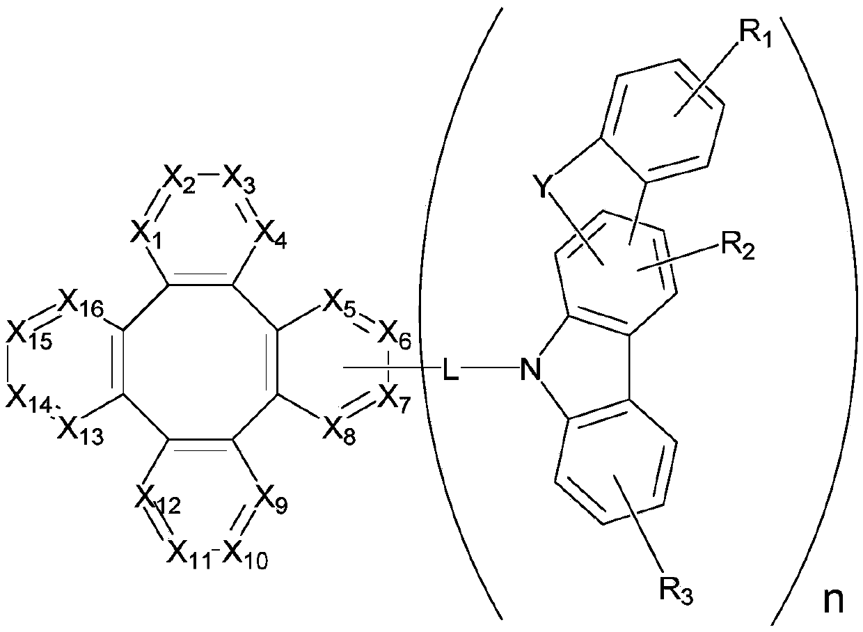
A compound, unsubstituted technology, applied in organic light-emitting devices, organic electroluminescent devices and compound formulations, in the field of compounds with indolecarbazole tetra-o-phenylene structure, can solve the problems that the application has not been widely developed, and achieve good devices performance effect
- Summary
- Abstract
- Description
- Claims
- Application Information
AI Technical Summary
Problems solved by technology
Method used
Image

Examples
Embodiment Construction
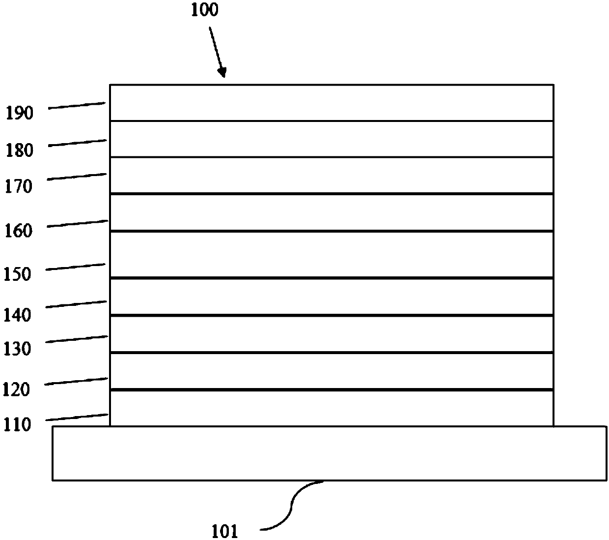
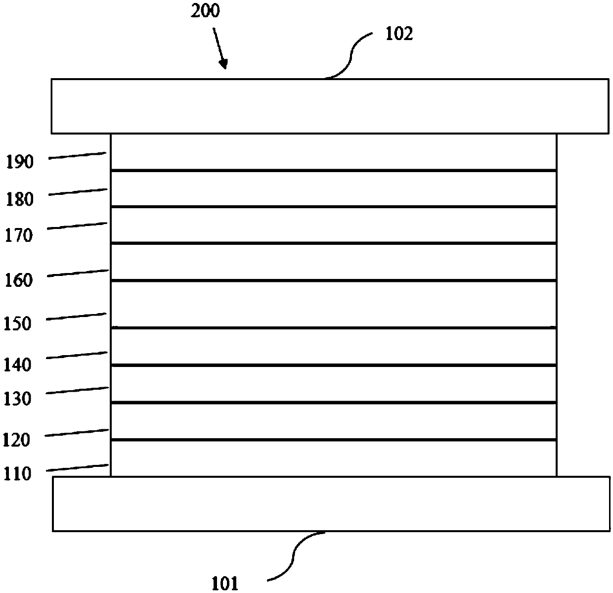
[0040] OLEDs can be fabricated on various substrates such as glass, plastic and metal. figure 1 The organic light emitting device 100 is shown schematically and non-limitatively. The drawings are not necessarily drawn to scale, and some layer structures in the drawings can also be omitted as needed. Device 100 may include substrate 101 , anode 110 , hole injection layer 120 , hole transport layer 130 , electron blocking layer 140 , light emitting layer 150 , hole blocking layer 160 , electron transport layer 170 , electron injection layer 180 and cathode 190 . Device 100 may be fabricated by sequentially depositing the described layers. The properties and functions of the various layers, as well as exemplary materials, are described in more detail in US Patent No. 7,279,704 B2, columns 6-10, the entire contents of which are incorporated herein by reference.
[0041] Each of these layers has more instances. For example, flexible and transparent substrate-anode combinations a...
PUM
| Property | Measurement | Unit |
|---|---|---|
| molecular weight | aaaaa | aaaaa |
Abstract
Description
Claims
Application Information