Electrolytic nickel (ALLOY) plating solution

A technology of plating solution and electrolytic nickel, applied in circuits, printed circuits, electrical components, etc., can solve the problems of poor structure, insufficient filling, insufficient filling of electrolytic nickel plating solution, etc., to increase the amount of nickel precipitation, The effect of firm engagement

Active Publication Date: 2019-07-09
JAPAN PURE CHEM
View PDF3 Cites 2 Cited by
  • Summary
  • Abstract
  • Description
  • Claims
  • Application Information

AI Technical Summary

Problems solved by technology

[0011] However, according to the further experiments of the present inventors (the examples described later), it can be known that the fillability of the electrolytic nickel plating solution described in Non-Patent Document 2 is still insufficient, and the generation of pores cannot be suppressed, and the formation of voids in the precipitates is still insufficient. Cracks, it can be seen that it is still bad as a structure
[0012] The miniaturization of electronic parts is progressing day by day. In this known technology, the fillability of tiny holes or tiny recesses is insufficient. It is expected to develop a nickel filling method that does not cause defects such as pores or cracks.

Method used


Image

  • Electrolytic nickel (ALLOY) plating solution
  • Electrolytic nickel (ALLOY) plating solution
  • Electrolytic nickel (ALLOY) plating solution

Examples


Embodiment 1 to 6、 comparative example 1 to 3

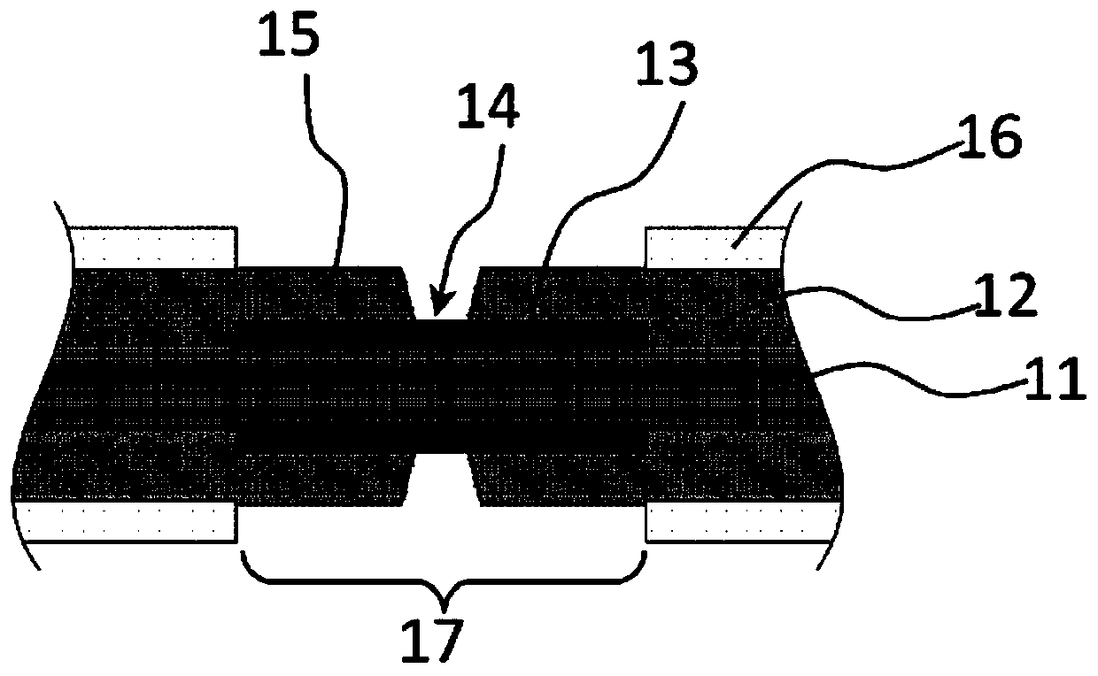
[0163] A 12 mm square evaluation printed circuit board (manufactured by Japan Circuit Co., Ltd.) having a laser guide hole with an aspect ratio of 0.88 (φ45 μm×40 μmD) was used as a model of the minute concave portion.

[0164] The sectional view of the periphery 10 of the plated part is as figure 1 shown. After attaching a copper foil 13 with a thickness of 12 μm to the via hole forming part of the substrate 11 made of BT (Bismaleimide-Triazine) with a thickness of 0.4 mm, a prepreg type build-up resin 12 with a thickness of 60 μm is laminated, and then laser Make a blind hole (hereinafter sometimes referred to as "conducting hole" or "guide hole") 14 with a diameter of 45 μm and a depth of 40 μm, and conduct electroless copper plating on the outer surface of the substrate (the surface of the build-up resin 12 ) and the guide hole 14 A seed layer 15 of about 1 μm is formed on the inner wall surface of the .

[0165] Then it is formed by a dry film photoresist (DFR: Dry Film...

Embodiment 7 to 8、 comparative example 4

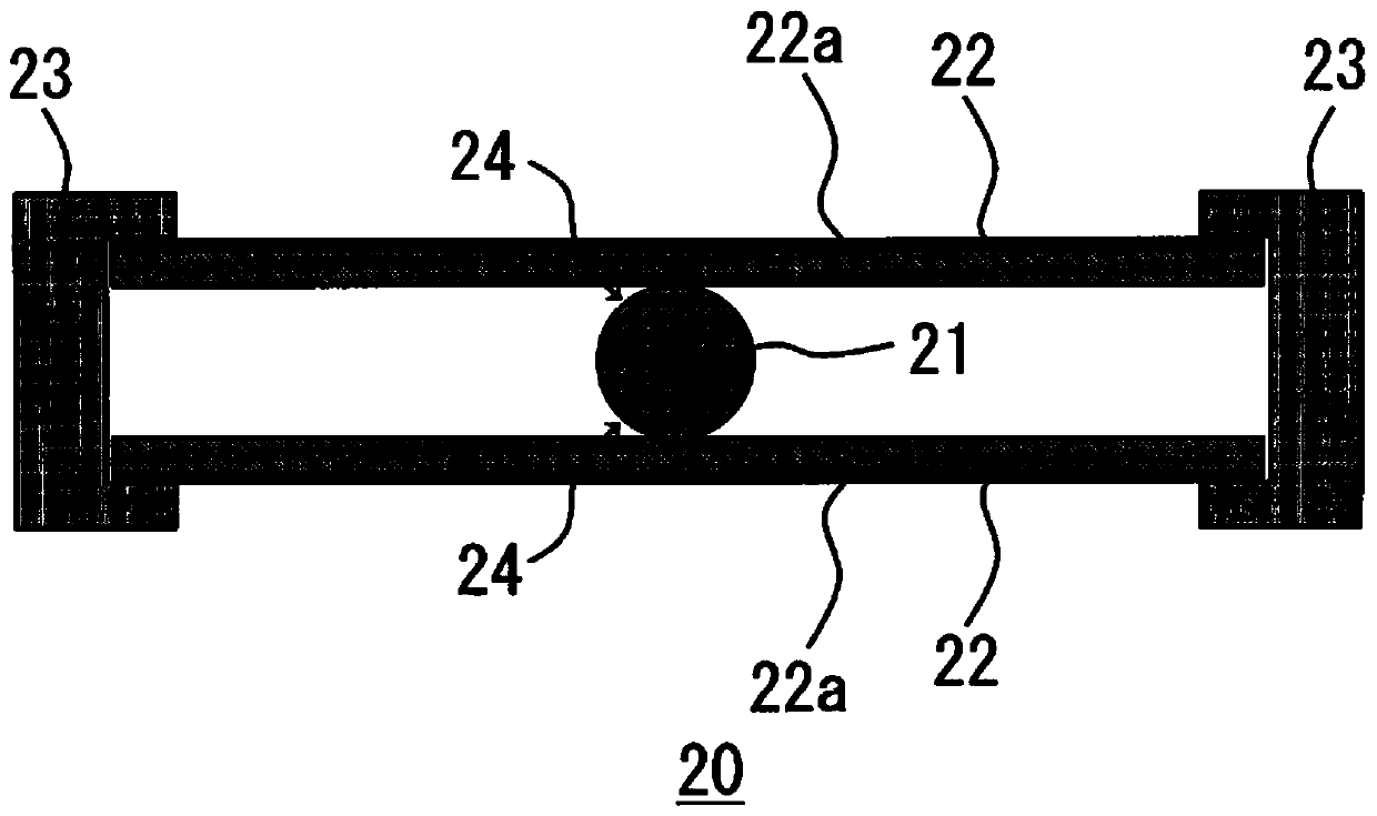
[0192] A copper wire (φ0.9mm) and a copper plate (20mm×20mm×0.3mmt) with a masked back surface were used as a model of the electronic component to be joined.

[0193] Such as image 3 As shown, prepare two copper plates 22 after shielding the back side by the masking material 22a, clamp the copper wire 21 with the unshielded surface of the two copper plates 22, and fix it with the auxiliary tool 23, and make the copper wire 21 and An electronic component sample 20 in which a minute gap 24 is formed between copper plates 22 .

[0194]

[0195] An electrolytic nickel plating solution was prepared by dissolving in deionized water so as to be 600 g / L of nickel sulfamate, 10 g / L of nickel chloride, and 30 g / L of boric acid, respectively.

[0196] The additives shown in Table 4 were added to the above-mentioned electrolytic nickel plating solution so as to be added in the amounts shown in Table 4, and dissolved.

[0197] Then, an appropriate amount of 100 g / L aqueous sulfamic ac...


PUM

PropertyMeasurementUnit
thicknessaaaaaaaaaa
thicknessaaaaaaaaaa

Abstract

The present invention addresses the problem of providing an electrolytic nickel (alloy) plating solution which is able to fill micro holes or micro recesses 14 within an electronic circuit component with nickel or nickel alloy 18 without the generation of defects such as voids and seams and firmly join two or more electronic components together by filling micro gaps. The present invention also addresses the problem of providing a nickel or nickel alloy plating / filling method with which an electrolytic nickel (alloy) plating solution is used, a method for producing a minute three-dimensional structure, an electronic component assembly, and a production method therefor. The problems have been solved by filling the micro holes or micro recesses 14 with an electrolytic nickel (alloy) plating solution which contains a specific N-substituted pyridinium compound.

Description

technical field [0001] The present invention relates to an electrolytic nickel plating solution or an electrolytic nickel alloy plating solution (hereinafter sometimes collectively referred to as "electrolytic nickel (alloy) plating solution". In addition, sometimes by using electrolytic nickel (alloy) plating solution precipitated "Nickel or nickel alloy" is referred to as "nickel (alloy)"). More specifically, it relates to plating and filling of tiny holes or tiny recesses in electronic parts, and when two or more electronic parts are stacked on top of each other. The electrolytic nickel (alloy) plating solution is filled in the plating of the generated minute gap. [0002] Furthermore, the present invention relates to a method of plating and filling microscopic holes or microscopic recesses using the electrolytic nickel (alloy) plating solution, a method of manufacturing a micro three-dimensional structure, an electronic component assembly, or the manufacturing method there...

Claims


Application Information

Patent Timeline
Patent Type & Authority Applications(China)
IPC IPC(8): C25D3/12C25D7/00
CPCC25D7/00C25D3/18C25D5/02C25D7/123C25D7/12C25D3/562H05K3/423H01L21/2885C25D3/12
Inventor 柴田和也大平原祐树
Owner JAPAN PURE CHEM
Why Eureka
Try Eureka