Display device
A technology for display equipment and data lines, which is applied to static indicators, identification devices, instruments, etc., and can solve problems such as the reduction of the display panel aperture ratio
- Summary
- Abstract
- Description
- Claims
- Application Information
AI Technical Summary
Problems solved by technology
Method used
Image

Examples
Embodiment 1
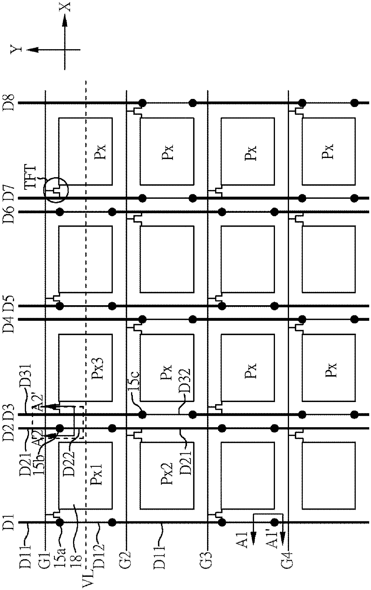
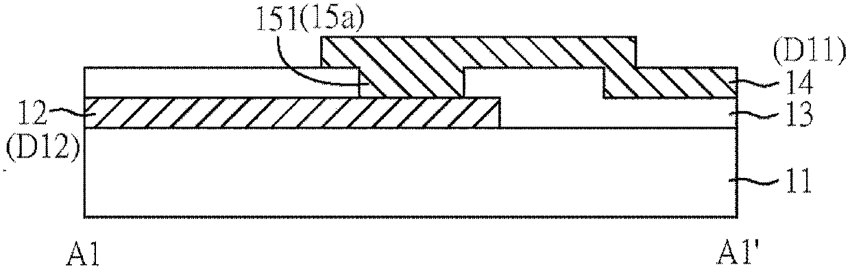
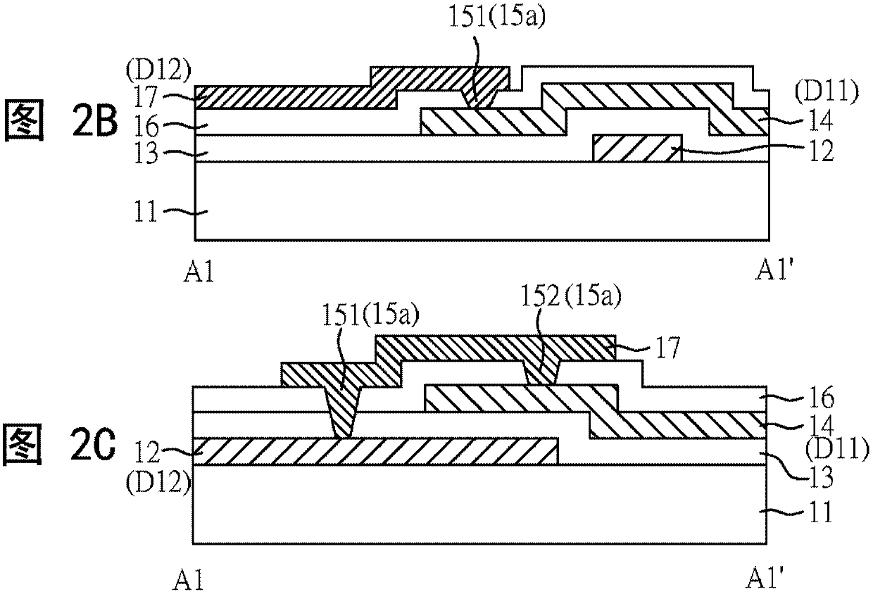
[0047] figure 1 is a top view of the display device of this embodiment. Figure 2A is the edge of the display device of this embodiment figure 1 The schematic cross-section of A1-A1'. The display device of this embodiment includes: a substrate 11; a first pixel unit Px1 and a second pixel unit Px2, disposed on the substrate 11, wherein the first pixel unit Px1 and the second pixel unit Px2 are arranged along a first direction Y Setting, in this embodiment, the first pixel unit Px1 is adjacent to the second pixel unit Px2, but not limited thereto; and a first data line D1 and a second data line D2 are arranged on the substrate 11, The first data line D1 and the second data line D2 respectively extend along the first direction Y, and the first data line D1 and the second data line D2 are arranged along a second direction X. In this embodiment, the first data line D1 and the second data line D2 are arranged parallel to the second direction X, but the present disclosure is not ...
Embodiment 2
[0073] Figure 7 is a top view of the display device of this embodiment. The display device of this embodiment is similar to that of Embodiment 1, the difference lies in that the third pixel unit Px3 and the transistor TFT corresponding to other pixel units marked with Px are connected to the data line differently from Embodiment 1. In more detail, the first data line D1, the second data line D2, the data line D5, and the data line D6 are correspondingly connected to the transistor TFT of the pixel unit in a manner similar to that of Embodiment 1, while the third data line D3, the data line D4, the data line D7, and the data line D8 are correspondingly connected to the transistor TFT of the pixel unit in a different manner from that of the first embodiment.
[0074] For example, if figure 1 As shown, in Embodiment 1, the transistor TFT of the third pixel unit Px3 is provided with a signal by the third data line D3. Such as Figure 7 As shown, in this embodiment, the transi...
Embodiment 3
[0076] Figure 8 is a top view of the display device of this embodiment. The display device of this embodiment is similar to that of Embodiment 1, and the differences are briefly described as follows.
[0077] In the display device of this embodiment, the second conductive segment D22 of the second data line D2 corresponds to the first pixel unit Px1, and the first conductive segment D11 of the first data line D1 corresponds to the first pixel unit Px1; the second The first conductive line segment D21 of the data line D2 is set corresponding to the second pixel unit Px2, the second conductive line segment D12 of the first data line D1 is set corresponding to the second pixel unit Px2; and the first conductive line segment D31 of the third data line D3 It is set corresponding to the third pixel unit Px3. More specifically, the two sides of the pixel electrode 18 of the first pixel unit Px1 are respectively, for example, the first conductive line segment D11 of the first data ...
PUM
| Property | Measurement | Unit |
|---|---|---|
| size | aaaaa | aaaaa |
| size | aaaaa | aaaaa |
| size | aaaaa | aaaaa |
Abstract
Description
Claims
Application Information