A kind of sbd device and preparation method thereof

A technology of devices and metal layers, which is applied in the field of SBD devices and its preparation, can solve the problems of unsatisfactory device breakdown voltage, large device leakage current, and limited device terminal electric field modulation, and achieve simple device structure and manufacturing process, Effect of reducing leakage current and enhancing electric field modulation

Active Publication Date: 2022-07-29
NO 55 INST CHINA ELECTRONIC SCI & TECHNOLOGYGROUP CO LTD
View PDF0 Cites 0 Cited by
  • Summary
  • Abstract
  • Description
  • Claims
  • Application Information

AI Technical Summary

Problems solved by technology

However, for the conventional field plate structure, its modulation effect on the terminal electric field of the device is limited, and the improvement of the breakdown voltage of the device is not ideal, and the highest electric field is distributed on the surface of the device, which easily causes a large leakage current of the device

Method used


Image

  • A kind of sbd device and preparation method thereof
  • A kind of sbd device and preparation method thereof
  • A kind of sbd device and preparation method thereof

Examples


Embodiment Construction

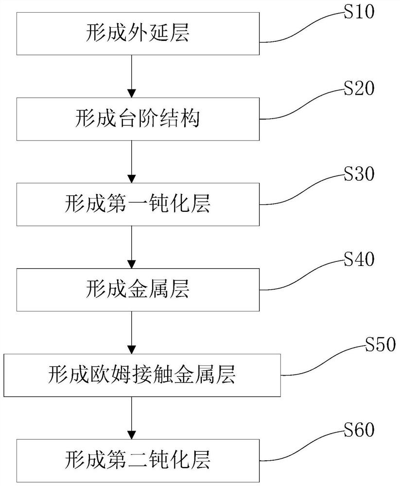
[0025] The technical solutions in the embodiments of the present invention will be clearly and completely described below with reference to the accompanying drawings in the embodiments of the present invention. Obviously, the described embodiments are only a part of the embodiments of the present invention, but not all of the embodiments. Based on the embodiments of the present invention, all other embodiments obtained by those skilled in the art without creative efforts shall fall within the protection scope of the present invention.

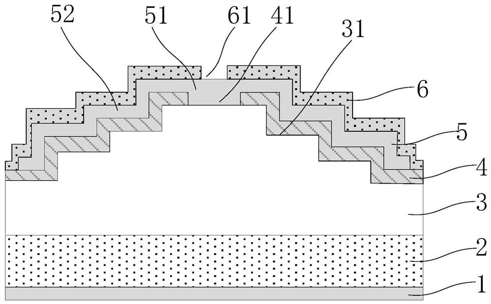
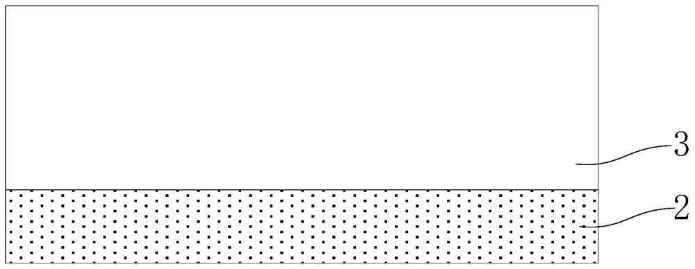
[0026] The embodiment of the present invention discloses an SBD device, such as figure 1 As shown, the SBD device includes: an ohmic contact metal layer 1 , a substrate 2 , an epitaxial layer 3 , a first passivation layer 4 , a metal layer 5 and a second passivation layer 6 .

[0027] The ohmic contact metal layer 1 is a Ti / Au double-layer metal, the thickness of the Ti layer is 10-40 nm, and the thickness of the Au layer is 50-150 nm. In this...


PUM

PropertyMeasurementUnit
thicknessaaaaaaaaaa
thicknessaaaaaaaaaa
breakdown field strengthaaaaaaaaaa

Abstract

The invention provides an SBD device and a preparation method thereof. The SBD device comprises: an ohmic contact metal layer; a substrate, located on the ohmic contact metal layer; an epitaxial layer, located on the substrate; a first passivation layer on the epitaxial layer; a metal layer on the first passivation layer; and a second passivation layer on the metal layer. An SBD device and a preparation method thereof provided by the present invention, through the vertical Ga 2 O 3 The multi-step field plate structure is introduced into the SBD device, which not only solves the electric field aggregation effect at the steps, improves the electric field modulation effect, and improves the breakdown voltage of the device, but also pulls the electric field peak value of the device from the surface to the device, reducing the leakage current of the device.

Description

technical field [0001] The invention relates to the technical field of semiconductors, in particular to an SBD device and a preparation method thereof. Background technique [0002] With the increasing energy crisis and the increasingly prominent environmental problems, technologies centered on energy conservation and emission reduction continue to emerge. Among them, the technical field of improving energy efficiency by improving the existing power system is the most concerned. According to statistics, 60% to 70% of the electrical energy is used in low energy consumption systems, and most of the energy consumption is wasted in power conversion and electric drive. Playing a key role in improving the efficiency of power utilization are power devices, also known as power electronic devices. How to reduce the energy consumption of power devices has become an important global issue. [0003] β-Ga 2 O 3 As a newly developed ultra-wide bandgap semiconductor material, the band ...

Claims


Application Information

Patent Timeline
Patent Type & Authority Patents(China)
IPC IPC(8): H01L29/872H01L29/40H01L21/34
CPCH01L29/872H01L29/402H01L29/66969
Inventor 王谦费晨曦柏松
Owner NO 55 INST CHINA ELECTRONIC SCI & TECHNOLOGYGROUP CO LTD
Why Eureka
Try Eureka