Semiconductor laser device and preparation method thereof

A laser device and semiconductor technology, which is applied in the direction of semiconductor lasers, laser components, lasers, etc., can solve problems such as damage to the cavity surface, achieve the effects of improving power and life, improving light extraction efficiency, and preventing optical catastrophe of the cavity surface

Inactive Publication Date: 2021-01-22
广东鸿芯科技有限公司
View PDF2 Cites 0 Cited by
  • Summary
  • Abstract
  • Description
  • Claims
  • Application Information

AI Technical Summary

Problems solved by technology

[0008] However, a cleaning step is required before the passivation film is prepared, which will cause certain damage to the cavity surface; the non-radiation absorption window technology will additionally prepare semiconductor materials

Method used


Image

  • Semiconductor laser device and preparation method thereof
  • Semiconductor laser device and preparation method thereof
  • Semiconductor laser device and preparation method thereof

Examples


Embodiment Construction

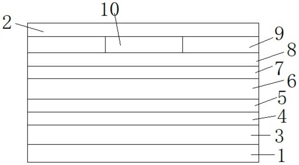
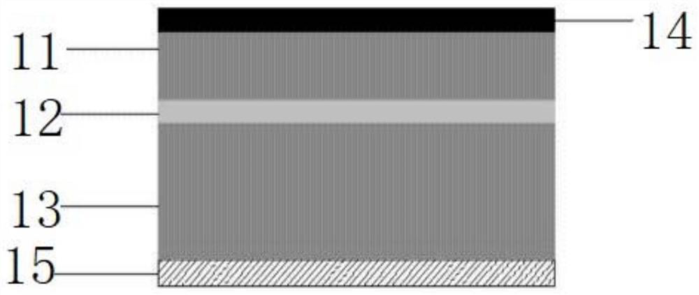
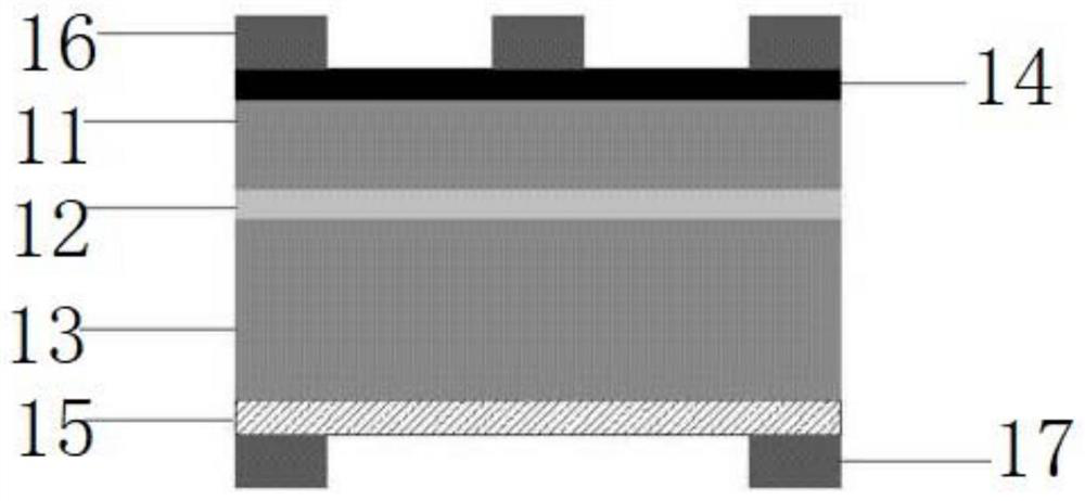
[0065] In order to make the purpose, technical solutions and advantages of the present disclosure clearer, the present disclosure will be further described in detail below in conjunction with specific embodiments.

[0066] It should be noted that, unless otherwise defined, the technical terms or scientific terms used in the embodiments of the present specification shall have ordinary meanings understood by those skilled in the art to which the present disclosure belongs. "First", "second" and similar words used in the embodiments of this specification do not indicate any sequence, quantity or importance, but are only used to distinguish different components. "Comprising" or "comprising" and similar words mean that the elements or items appearing before the word include the elements or items listed after the word and their equivalents, without excluding other elements or items. Words such as "connected" or "connected" are not limited to physical or mechanical connections, but m...


PUM

PropertyMeasurementUnit
thicknessaaaaaaaaaa
thicknessaaaaaaaaaa
thicknessaaaaaaaaaa

Abstract

The invention provides a semiconductor laser device and a preparation method thereof. The semiconductor laser device comprises a first electrode, a second electrode, and a substrate, a first limitinglayer, a first waveguide layer, an active region, a second waveguide layer, a second limiting layer, an ohmic contact layer and a transmission grating layer which are arranged between the first electrode and the second electrode and are sequentially arranged from the first electrode to the second electrode, wherein the transmission grating layer is in contact with the second limiting layer. The transmission grating layer is arranged between a P-surface electrode and a P-type limiting layer, so that the high resolution of the semiconductor laser is improved, and the semiconductor laser has theadvantage of high light beam quality. And the requirements of large effective area and smooth side wall of the X-ray self-supporting blazed transmission grating can be met at the same time.

Description

technical field [0001] The invention relates to the technical field of semiconductor optoelectronics, in particular to a semiconductor laser device and a preparation method thereof. Background technique [0002] With the development of laser technology, a new applied discipline - laser medicine has gradually formed. The unique advantages of laser have solved many problems that traditional medicine cannot solve in basic research and clinical application, and have attracted the attention of domestic and foreign medical circles. Semiconductor lasers (DL) are especially suitable for the manufacture of medical equipment due to their small size, light weight, long life, low power consumption, and wide wavelength coverage. In addition, semiconductor lasers are widely used in important fields such as optical fiber communication, optical disk access, spectral analysis and optical information processing. [0003] X-ray self-supporting blazed transmission gratings have huge applicatio...

Claims


Application Information

Patent Timeline
Patent Type & Authority Applications(China)
IPC IPC(8): H01S5/12H01S5/028
CPCH01S5/028H01S5/0282H01S5/1206H01S2301/17
Inventor 毛虎毛森焦英豪陆凯凯毛融田
Owner 广东鸿芯科技有限公司
Why Eureka
Try Eureka