

Chip with memory
A chip and switching circuit technology, applied in the architecture with a single central processing unit, general-purpose stored program computer, software deployment, etc., can solve the problem of limited transmission speed, communication interface transmission speed, etc.
- Summary
- Abstract
- Description
- Claims
- Application Information
AI Technical Summary
Problems solved by technology
Method used
Image

Examples
Embodiment Construction
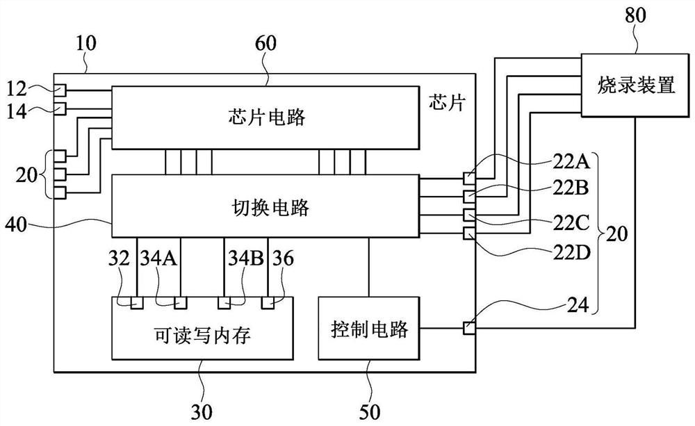
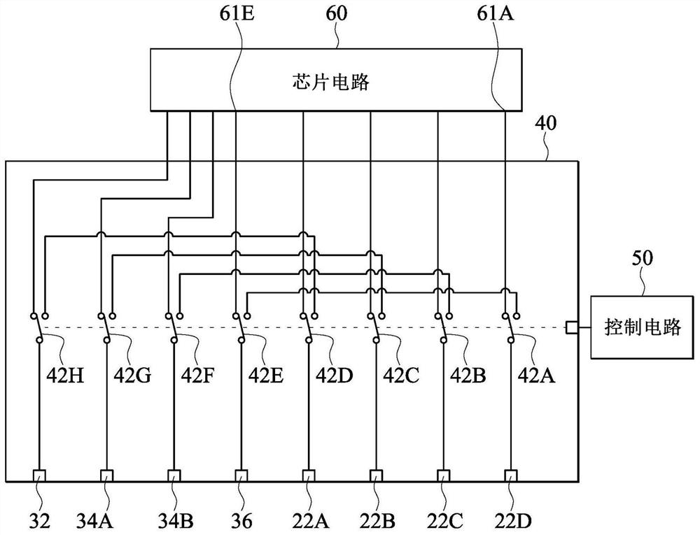
[0015] refer to figure 1 , figure 1 A block schematic diagram of a chip 10 according to some embodiments is shown. The chip 10 includes a power pin 12 , a ground pin 14 , a plurality of input and output pins 20 , a readable and writable memory 30 , a switching circuit 40 , and a control circuit 50 . The input and output pins 20 include a plurality of mapping pins 22A˜ 22D and a control pin 24 . The readable and writable memory 30 includes a frequency port 32 , a plurality of input and output ports 34A˜ 34B, and an enable port 36 . The control circuit 50 activates or deactivates the switching circuit 40 according to the control pin 24 . When the switching circuit 40 is activated, the switching circuit 40 electrically connects the frequency port 32 , the input / output ports 34A- 34B, and the enabling port 36 to the mapping pins 22A- 22D respectively.
[0016] Therefore, the burning device 80 controls the pin 24 to make the control circuit 50 actuate the switching circuit 40. ...
PUM
 Abstract
Description
Claims
Application Information