Special-shaped display panel, display device and preparation method of display panel
A display panel and special-shaped technology, which is used in identification devices, nonlinear optics, instruments, etc., can solve the problems of poor edge jaggedness and poor color dots in the display area of the special-shaped display panel, and reduce or eliminate jaggedness and color. Bad dots, bad anti-aliasing, good display effect
- Summary
- Abstract
- Description
- Claims
- Application Information
AI Technical Summary
Problems solved by technology
Method used
Image
Examples
Embodiment 1
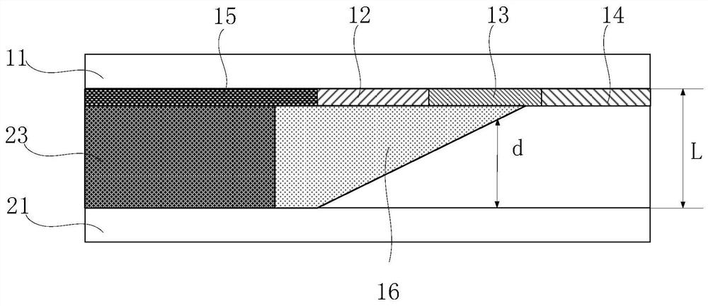
[0059] Such as image 3 and Figure 5 As shown, in the special-shaped display panel provided in this embodiment, the transparent filling layer includes a first transparent filling structure 16 , and the first transparent filling structure 16 is disposed on the color filter substrate and extends toward the direction close to the array substrate 21 . Specifically, the first transparent filling structure 16 is made of a transparent insulating material, and a first slope can be formed on the side facing the array substrate 21 through an etching process, so that the thickness of the first transparent filling structure 16 is determined by the thickness of the non-display area. The opposite end gradually decreases towards the other end.
[0060] exist image 3 Among them, the color filter substrate of the special-shaped display panel includes a first substrate 11, and edge pixel units are arranged on the first substrate 11, one edge pixel unit includes one edge pixel, and one edge ...
Embodiment 2
[0063] Such as Figure 6 As shown, in the special-shaped display panel provided in this embodiment, the transparent filling layer includes a second transparent filling structure 22, and the second transparent filling structure 22 is disposed on the array substrate 21 and extends toward the color filter substrate.
[0064] Specifically, the second transparent filling structure 22 is made of a transparent insulating material, and a second slope can be formed on the side facing the array substrate 21 through an etching process, so that the thickness of the second transparent filling structure 22 is determined by the thickness of the non-display area. The opposite end gradually decreases towards the other end.
[0065] exist Figure 6 Among them, the color filter substrate of the special-shaped display panel includes a first substrate 11, and edge pixel units are arranged on the first substrate 11, one edge pixel unit includes one edge pixel, and one edge pixel includes three edg...
Embodiment 3
[0067] Such as Figure 7 As shown, in the special-shaped display panel provided in this embodiment, the transparent filling layer includes a first transparent filling structure 16 and a second transparent filling structure 22, the first transparent filling structure 16 is arranged on the color filter substrate, and the second transparent filling structure 22 Located on the array substrate 21 , a partial area of the first transparent filling structure 16 is in contact with a partial area of the second transparent filling structure 22 .
[0068] exist Figure 7 Among them, the color filter substrate of the special-shaped display panel includes a first substrate 11, and edge pixel units are arranged on the first substrate 11, one edge pixel unit includes one edge pixel, and one edge pixel includes three edge sub-pixels, which are respectively the first A sub-pixel 12 , a second sub-pixel 13 and a third sub-pixel 14 . One of the first sub-pixel 12 , the second sub-pixel 13 a...
PUM
 Abstract
Description
Claims
Application Information


