A lateral double diffused transistor

A lateral double-diffusion and transistor technology, applied in diodes, semiconductor devices, electric solid-state devices, etc., can solve problems such as device damage, achieve the effects of avoiding non-uniform opening, realizing anti-ESD ability, and improving anti-ESD ability

Active Publication Date: 2022-05-10
JOULWATT TECH INC LTD
View PDF6 Cites 0 Cited by
  • Summary
  • Abstract
  • Description
  • Claims
  • Application Information

AI Technical Summary

Problems solved by technology

[0006] The purpose of the present invention is to provide a lateral double-diffused transistor, which is used to overcome the damage caused by non-uniform turn-on of the device when ESD pours in from the drain in the prior art, so as to improve the ESD resistance of the device

Method used


Image

  • A lateral double diffused transistor
  • A lateral double diffused transistor
  • A lateral double diffused transistor

Examples


Embodiment Construction

[0029] The present invention will be described in detail below in conjunction with various embodiments, but it should be noted that these embodiments are not limitations of the present invention, and those of ordinary skill in the art can make functional, method, or structural equivalent transformations or replacements based on these embodiments. , all fall within the protection scope of the present invention.

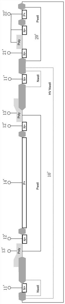
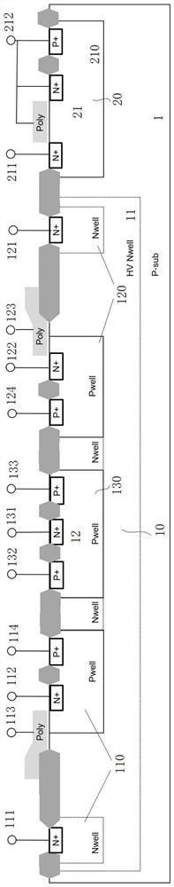
[0030] Such as image 3 As shown, an embodiment of the present invention provides a lateral double-diffused transistor, which includes: a substrate 1, a main part region 10 disposed on the substrate 1, and a main part region 10 also disposed on the substrate 1 and located in the main part region 10. Side accessories area 20. In the illustration, the accessory area 20 is located on the right side of the main area 10 , and in other implementations, the accessory area 20 can also be located on the left side of the main area 10 .

[0031] The master region 10 includes a ...


PUM


Abstract

The present invention provides a lateral double-diffusion transistor, the main part region of the lateral double-diffusion transistor includes a first transistor, a second transistor and a first ESD device arranged between the first transistor and the second transistor; the first transistor A transistor and a second transistor have a common source terminal, a common drain terminal, a common gate terminal and a common body terminal; the first ESD device includes a cathode connected to the common gate terminal , and two positive poles arranged on the left and right sides of the negative pole, the two positive poles are connected to the common source terminal; the secondary part area includes a second ESD device, and the input of the second ESD device The terminal is connected to the common gate terminal, and the output terminal is grounded. The invention can overcome the damage caused by non-uniform turn-on of the device when ESD surges from the drain end in the prior art, so as to improve the ESD prevention capability of the device.

Description

technical field [0001] The invention relates to the technical field of semiconductors, in particular to a lateral double-diffusion transistor. Background technique [0002] In semiconductor power devices, MOS devices occupy an important position, among which double-diffused metal oxide semiconductor field effect transistor (Double-Diffused MOSFET, referred to as DMOS) is one of the most commonly used forms of power devices, DMOS devices are mainly divided into two types Types, vertical DMOS (referred to as VDMOS) and horizontal DMOS (referred to as LDMOS). LDMOS devices are voltage-controlled devices. Compared with bipolar devices, they have the advantages of high withstand voltage, high input impedance, good safe working area, and low power consumption. They are generally used in motor drives, automotive electronics, industrial control, and switches. It is used as a high-voltage power device in the power supply circuit. [0003] Ultra High Voltage Lateral Double Diffused ...

Claims


Application Information

Patent Timeline
Patent Type & Authority Patents(China)
IPC IPC(8): H01L29/78H01L27/02
CPCH01L29/7816H01L29/7818H01L27/0251
Inventor 韩广涛王炜槐
Owner JOULWATT TECH INC LTD
Why Eureka
Try Eureka