

NOR flash memory manufacturing method, circuit and application thereof
A manufacturing method and flash memory technology, applied in circuits, electrical components, electrical solid state devices, etc., can solve the problems of inability to meet the needs of complex circuits and more aluminum pad wiring, inability to meet the needs of metal wiring, and high production costs. The effect of photolithography and etching accuracy, short cycle and low production cost
- Summary
- Abstract
- Description
- Claims
- Application Information
AI Technical Summary
Problems solved by technology
Method used
Image

Examples
Embodiment 1
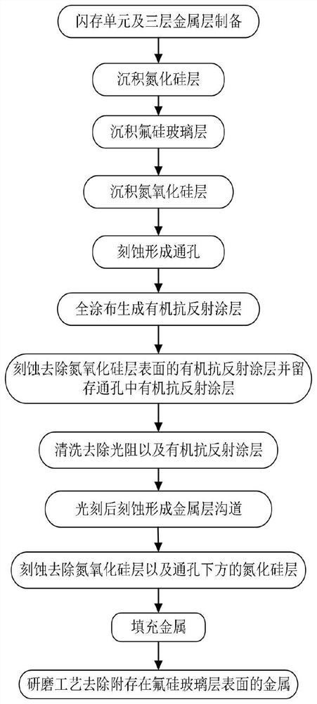
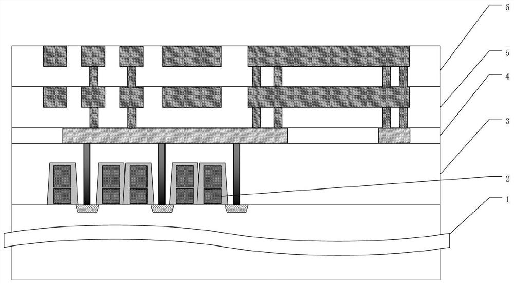
[0041] Such as Figure 1-11 As shown, the manufacturing method of a kind of NOR flash memory that this embodiment provides, please refer to figure 1 Since this method includes using the existing process to prepare flash memory unit 2 on silicon wafer substrate 1, covering and preparing inner layer insulating layer 3 on flash memory unit 2, and covering and preparing first metal Layer 4, the second metal layer 5 and the third metal layer 6, such as the deposition of tunnel oxide layer and floating gate included in the preparation of flash memory unit 2, etching of the floating gate, tunnel oxide layer and silicon wafer substrate to form shallow trenches The tank may also contain the exposure and development, ion implantation, ashing, and cleaning steps included in the zero-threshold voltage tube ion implantation process disclosed in the applicant's previous patent application. Therefore, in the embodiment, the same steps as those in the prior art And the parameters will not be...
Embodiment 2
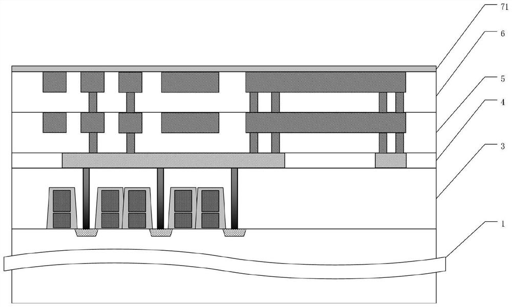
[0053] This implementation provides a NOR flash memory circuit, including a wafer of a Nor flash memory circuit provided with a flash memory unit and three metal layers, and also includes a fourth metal layer prepared by the method as in Example 1 on the surface of the wafer.
Embodiment 3
[0055] This embodiment provides a chip, including the NOR flash memory circuit described in Embodiment 2.
PUM
 Abstract
Description
Claims
Application Information