Photosensitive circuit structure and optical device

A technology of circuit structure and photosensitive unit, applied in electrical components, components of color TV, components of TV system, etc., to achieve the effect of improving signal-to-noise ratio, reducing leakage current and improving working performance

Pending Publication Date: 2022-04-15
HEFEI VISIONOX TECH CO LTD
View PDF0 Cites 1 Cited by
  • Summary
  • Abstract
  • Description
  • Claims
  • Application Information

AI Technical Summary

Problems solved by technology

[0003] However, the image quality of existing X-Ray flat panel detectors still needs to be further improved, which is also an important subject of continuous research in the industry

Method used


Image

  • Photosensitive circuit structure and optical device
  • Photosensitive circuit structure and optical device
  • Photosensitive circuit structure and optical device

Examples


Embodiment Construction

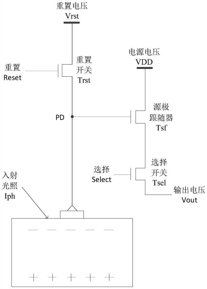
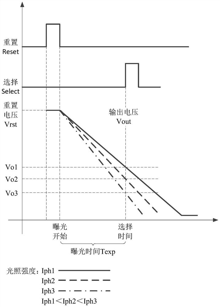
[0055] In the related art, the photosensitive circuit structure of the pixel of the image detector usually includes a plurality of transistors. The following describes in detail in conjunction with the equivalent circuit diagram of the photosensitive circuit structure with three transistors and its working timing diagram. figure 1 It is an equivalent circuit diagram of the photosensitive circuit structure provided in the related art, figure 2 for figure 1 The working timing diagram of the equivalent circuit diagram of the photosensitive circuit structure. refer to figure 1 As shown, the equivalent circuit of the photosensitive circuit structure in the related art includes a reset switch transistor Trst, a source follower transistor Tsf, a selection switch transistor Tsel and a photodiode PD.

[0056] The input terminal of the reset switch transistor Trst is electrically connected to the reset voltage Vrst, the output terminal of the reset switch transistor Trst is electric...


PUM


Abstract

The invention provides a photosensitive circuit structure and an optical device. The photosensitive circuit structure comprises a photosensitive unit, a signal amplification unit and a control unit, the photosensitive unit comprises a photodiode and a reset transistor, the signal amplification unit comprises an amplification transistor, and the control unit comprises a control transistor; the input end of the reset transistor is electrically connected with the power supply end, the output end is electrically connected with the control end of the amplification transistor, and the control end is electrically connected with the reset signal end; the input end of the amplification transistor is electrically connected with the power supply end, the output end is electrically connected with the input end of the control transistor, and the control end is electrically connected with the control signal end; the leakage current of the reset transistor and the control transistor is smaller than the leakage current of the amplification transistor. The carrier mobility of the reset transistor is smaller than the carrier mobility of the amplification transistor and the carrier mobility of the control transistor. The leakage current of the photosensitive circuit structure is reduced, and the signal-to-noise ratio of signal transmission in the photosensitive circuit structure is improved, so that the performance of an optical device is improved.

Description

technical field [0001] The present application relates to the technical field of semiconductors, in particular to a photosensitive circuit structure and an optical device. Background technique [0002] With the development of semiconductor technology, X-Ray flat panel detectors have been widely used in medical testing, safety inspection, and industrial production. The X-Ray flat panel detector uses transistor array technology to form a pixel array on the substrate, and a layer of coating that can convert X-rays into visible light, such as a fluorescent film or a flash film, is placed above the pixel array. In the related art, each pixel of the X-Ray flat panel detector includes a photoelectric conversion unit and a transistor switch. In specific applications, X-rays are received by the X-Ray flat panel detector after passing through the irradiated object and converted into image output. [0003] However, the image quality of the existing X-Ray flat panel detector still nee...

Claims


Application Information

Patent Timeline
Patent Type & Authority Applications(China)
IPC IPC(8): H04N5/378H01L27/146
CPCH01L27/146
Inventor 任庆荣邢汝博李俊峰王刚崔霜张豪峰郭瑞孙丹丹
Owner HEFEI VISIONOX TECH CO LTD
Why Eureka
Try Eureka