Nanofluidic chip based on nanocracks and processing method thereof

A processing method and nanofluidic technology, applied in chemical instruments and methods, laboratory containers, laboratory utensils, etc., can solve the problem of poor processing repeatability, complex calibration and assembly process, and difficulty in meeting the mass production of microfluidic chips. To achieve high repeatability and good results

Pending Publication Date: 2022-05-06
DALIAN MARITIME UNIVERSITY
View PDF4 Cites 0 Cited by
  • Summary
  • Abstract
  • Description
  • Claims
  • Application Information

AI Technical Summary

Problems solved by technology

[0003] At present, the conventional processing of nanofluidic chips containing nanochannels still adopts traditional semiconductor processing techniques, such as electron beam lithography, focused ion beam lithography, dry and wet etching, etc., but these methods are still affected by incident light to varying degrees. and photomask resolution limitations, and its high processing cost, strict requirements on the processing environment, low processing efficiency, etc.; new processing technologies such as interference lithography do not need to use complex optical systems or photomasks to achieve large-area Fabricate simple periodic nanoscale structures, but this method cannot realize the prep

Method used


Image

  • Nanofluidic chip based on nanocracks and processing method thereof
  • Nanofluidic chip based on nanocracks and processing method thereof
  • Nanofluidic chip based on nanocracks and processing method thereof

Examples


Embodiment Construction

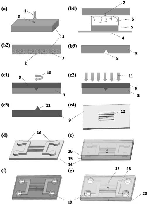
[0049] In order to make the purposes, technical solutions and advantages of the embodiments of the present invention clearer, the technical solutions in the embodiments of the present invention will be clearly and completely described below with reference to the accompanying drawings in the embodiments of the present invention. Obviously, the described embodiments These are some embodiments of the present invention, but not all embodiments. Based on the embodiments of the present invention, all other embodiments obtained by those of ordinary skill in the art without creative efforts shall fall within the protection scope of the present invention.

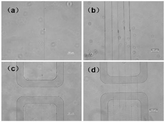
[0050] The invention discloses a nanofluidic chip based on nano cracks and a processing method thereof. The micro-nanofluidic chip is based on polydimethylsiloxane (polydimethylsilocane-PDMS) material; the chip contains a single micron channel and a nanochannel or a nanometer channel. Channel array; nanochannels are connected to the...


PUM

PropertyMeasurementUnit
Thicknessaaaaaaaaaa
Thicknessaaaaaaaaaa
Thicknessaaaaaaaaaa

Abstract

The invention provides a nanofluidic chip based on nanocracks and a processing method thereof. The nano-fluidic chip is formed by bonding a polydimethylsiloxane channel layer and a glass substrate, the polydimethylsiloxane channel layer contains a micron channel and at least one nano channel, the nano channel is connected with the micron channel, the tail end of the micron channel is connected with the outside through a liquid storage tank, and the liquid storage tank is used for adding and extracting a nano-fluidic chip sample. The processing method is simple, efficient and rapid processing of a single nano-channel array or a multi-nano-channel array can be achieved, and the length, the position and the size of the nano-channel are accurate and controllable. The problems of long time consumption, high cost, complex operation and the like of a traditional semiconductor processing technology are solved. The processed micro-nano fluidic chip can be used in the fields of biosensing, chemical analysis, micro-nano energy collection and the like based on the nanofluidic technology.

Description

technical field [0001] The invention relates to the field of micro-nano fluidic chip processing, in particular to a nano-crack-based nanofluidic chip and a processing method thereof. The processed micro-nanofluidic chip can be used in fields such as biosensing, chemical analysis, and micro-nano energy collection based on nanofluidic technology. Background technique [0002] Nanofluidic technology studies the transmission, manipulation mechanism and application technology of nanoscale substances such as nanoparticles, small molecules, ions, drug macromolecules, etc. in a space with a scale smaller than 100nm. Nanochannel devices with a structure size of less than 100nm will have many new transport phenomena in the transport of substances in nanopores due to interface electrical phenomena, size steric effects, etc. These new transport phenomena are useful for detecting, manipulating and controlling single nanoscale targets such as Viruses, bacteria, and DNA provide great poss...

Claims


Application Information

Patent Timeline
IPC IPC(8): B01L3/00
CPCB01L3/5027B01L3/502707B01L2300/0861B01L2300/12
Inventor 彭冉宋涵琼宋永欣李刚潘新祥李冬青
Owner DALIAN MARITIME UNIVERSITY
Why Eureka
Try Eureka