Display cover plate
A cover and light-transmitting layer technology, which is applied in the direction of identification devices, instruments, light guides, etc., can solve the problems of increased man-hours or cost of display cover assembly, space occupation, and increased thickness of the display cover.
- Summary
- Abstract
- Description
- Claims
- Application Information
AI Technical Summary
Problems solved by technology
Method used
Image

Examples
Embodiment Construction
[0039] The technical solution of the present invention will be described in detail below in conjunction with the accompanying drawings and specific embodiments to further understand the purpose, solution and effect of the present invention, but it is not intended to limit the scope of protection of the appended claims of the present invention.
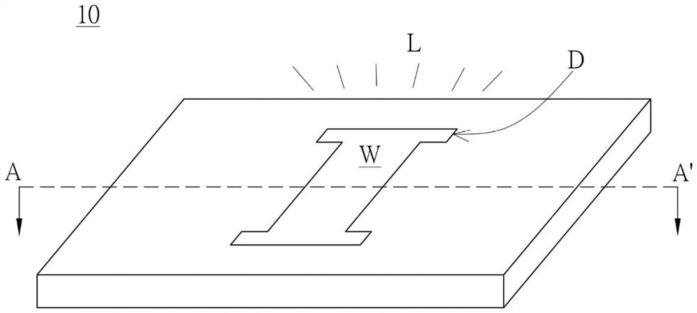
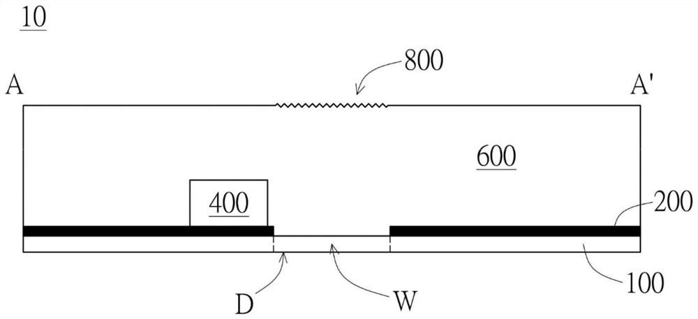
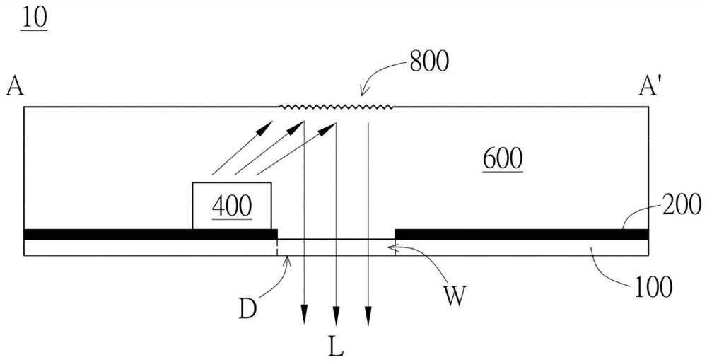
[0040] refer to figure 1 and figure 2 , which respectively show a schematic perspective view and a schematic cross-sectional view of the display cover 10 according to an embodiment of the present invention. Wherein, the display cover 10 is used for displaying a predetermined pattern D. As shown in FIG. The predetermined pattern D can be any text, figure, or image, and the I letter shown here is only a simple example, and the present invention is not limited thereto. As mentioned above, the display cover 10 can display the predetermined pattern D by emitting light L through the light-transmitting window W of the predetermined pattern...
PUM
 Abstract
Description
Claims
Application Information
PatSnap Eureka turns technology decisions into work you can execute. Powered by our Innovation Knowledge Graph, it runs expert workflows across engineering, life sciences, materials and intellectual property. Get your review-ready output in minutes.


