Supercharge Your Innovation With Domain-Expert AI Agents!

Handling method of changing attributes of manufacturing processes for semi-conductor equipment

A manufacturing process and semiconductor technology, applied in semiconductor/solid-state device manufacturing, memory systems, electrical digital data processing, etc., can solve problems such as inability to distinguish whether the attributes of the equipment manufacturing process have changed, polluting products, and increasing manufacturing costs

Inactive Publication Date: 2004-12-01
MACRONIX INT CO LTD
View PDF0 Cites 0 Cited by
  • Summary
  • Abstract
  • Description
  • Claims
  • Application Information

AI Technical Summary

Problems solved by technology

In the traditional semiconductor control system, the operation interface (OPI) cannot distinguish whether the manufacturing process attributes of the equipment have changed, so it cannot prevent the occurrence of different manufacturing process attributes in the same equipment
In this way, if there is a product during the manufacturing period, due to human negligence, the manufacturing process before the property of the equipment has been changed due to human error will cause serious pollution and cause the product to be scrapped, resulting in a substantial increase in manufacturing costs

Method used


Image

  • Handling method of changing attributes of manufacturing processes for semi-conductor equipment
  • Handling method of changing attributes of manufacturing processes for semi-conductor equipment
  • Handling method of changing attributes of manufacturing processes for semi-conductor equipment

Examples


Embodiment Construction

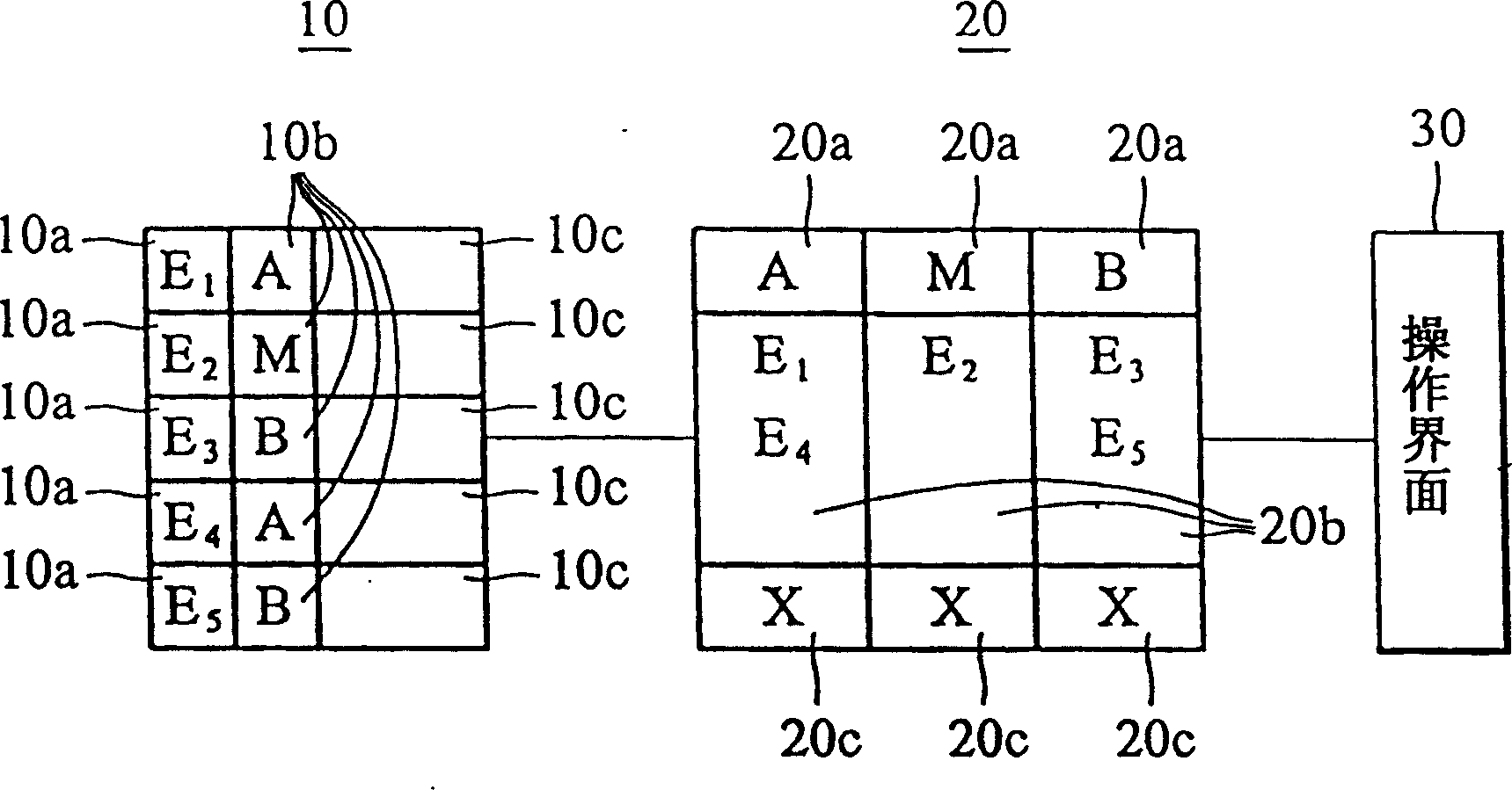
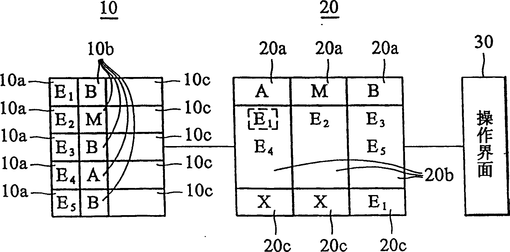
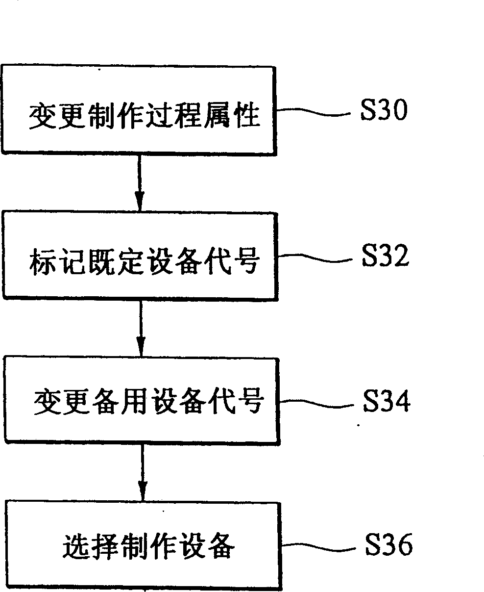
[0017] The following fit Figure 1 to Figure 3 The semiconductor manufacturing process control system and the method for handling the change of the manufacturing process attribute of the semiconductor equipment according to the embodiment of the present invention are described.

[0018] figure 1 It is a schematic diagram of a semiconductor manufacturing process control system according to an embodiment of the present invention. The system is used to process the change of manufacturing process attributes of multiple semiconductor devices, and at least includes an equipment data module 10 , a manufacturing process data module 20 and an operation interface 30 . The device data module 10 is used to store a plurality of device codes 10a (for example, E 1 ,E 2 ,E 3 ,E 4 ,E 5 ), a plurality of manufacturing process attribute data 10b (for example, A, M, B, A, B) corresponding to these equipment codes 10a, and a plurality of equipment data 10c corresponding to these equipment co...


PUM


Abstract

A method is suitable for the system for controlling manufacturing processes of semi-conductor. The system at least includes the device data module storing attribute data of multiple manufacturing processes and the data module of the manufacturing processes storing the manufacturing process data relevant to the attribute data. Moreover, each manufacturing process data possesses at least, one established device code name. First, one attribute data of manufacturing process is changed to another attirubte data of manufacturing process. Then, the established device code name in the manufacturing process data located before the attribute data of manufacturing process is changed to the marker denoting the invalid device code name. The operation interface of the control system is unable to select the invalid device code name so as to prevent metallic cross contamination happened to chips in the device.

Description

technical field [0001] The invention relates to a semiconductor manufacturing process, in particular to a method for dealing with semiconductor equipment changing manufacturing process attributes, so as to prevent chips from being scrapped due to metal cross-contamination in devices with different manufacturing process attributes. Background technique [0002] In the complex semiconductor manufacturing process, the manufacturing process is generally divided into three attributes: front-end, middle-end, and back-end. The manufacturing process procedures (recipes) used in each manufacturing process attribute are different and the required cleanliness is also different. Generally speaking, the cleanliness of the front-end manufacturing process is high, while the cleanliness of the back-end manufacturing process is low due to the presence of metal impurities, so each manufacturing process attribute must have dedicated manufacturing process equipment, such as deposition equipment,...

Claims


Application Information

Patent Timeline
Patent Type & Authority Patents(China)
IPC IPC(8): G06F9/00H01L21/00
Inventor 彭瑞珍顾宪国赖孟正马思尊
Owner MACRONIX INT CO LTD
Features
  • R&D
  • Intellectual Property
  • Life Sciences
  • Materials
  • Tech Scout
  • Unparalleled Data Quality
  • Higher Quality Content
  • 60% Fewer Hallucinations
Learn More