
Method of manufacturing pattern substrate and method of locating component

a technology of pattern substrate and manufacturing method, which is applied in the direction of soldering apparatus, instruments, photomechanical apparatus, etc., can solve the problems of residual magnetic force generation, heat disadvantage, and component vulnerable to heat, and achieve the effect of high accuracy

Active Publication Date: 2018-06-26
KONICA MINOLTA INC
View PDF3 Cites 0 Cited by
  • Summary
  • Abstract
  • Description
  • Claims
  • Application Information

AI Technical Summary

Benefits of technology

[0014]Another object of the present invention is to provide a method in which even a minute component can be highly accurately located on a substrate.

Problems solved by technology

However, with respect to the magnetic force, noise may be produced by a residual magnetic force.
Although advanced researches are conducted on the method utilizing the surface tension of a molten solder, and thus its practicality is high, a component vulnerable to heat cannot be used.
In addition, a residual stress is disadvantageously produced by heat.
Since in the method in which photolithography, etching and the like are used to perform patterning, it is necessary to use a mask or a plate, when the pattern is changed, time and money are disadvantageously needed.
As a method of facilitating the change of the pattern, a method of controlling a liquid by arranging devices for generating electric and magnetic fields in a grid is proposed; however, disadvantageously, it is impossible to obtain only the accuracy of the locating lower than the size of the grid which can be produced, and as the region which can be controlled is made larger, the size of the device (circuit) is increased.

Method used


Image

  • Method of manufacturing pattern substrate and method of locating component
  • Method of manufacturing pattern substrate and method of locating component
  • Method of manufacturing pattern substrate and method of locating component

Examples


Embodiment Construction

[0045]A method of manufacturing a pattern substrate and a method of locating a component according to the present invention will be described below with reference to accompanying drawings; the present invention is not limited at all to these embodiments.

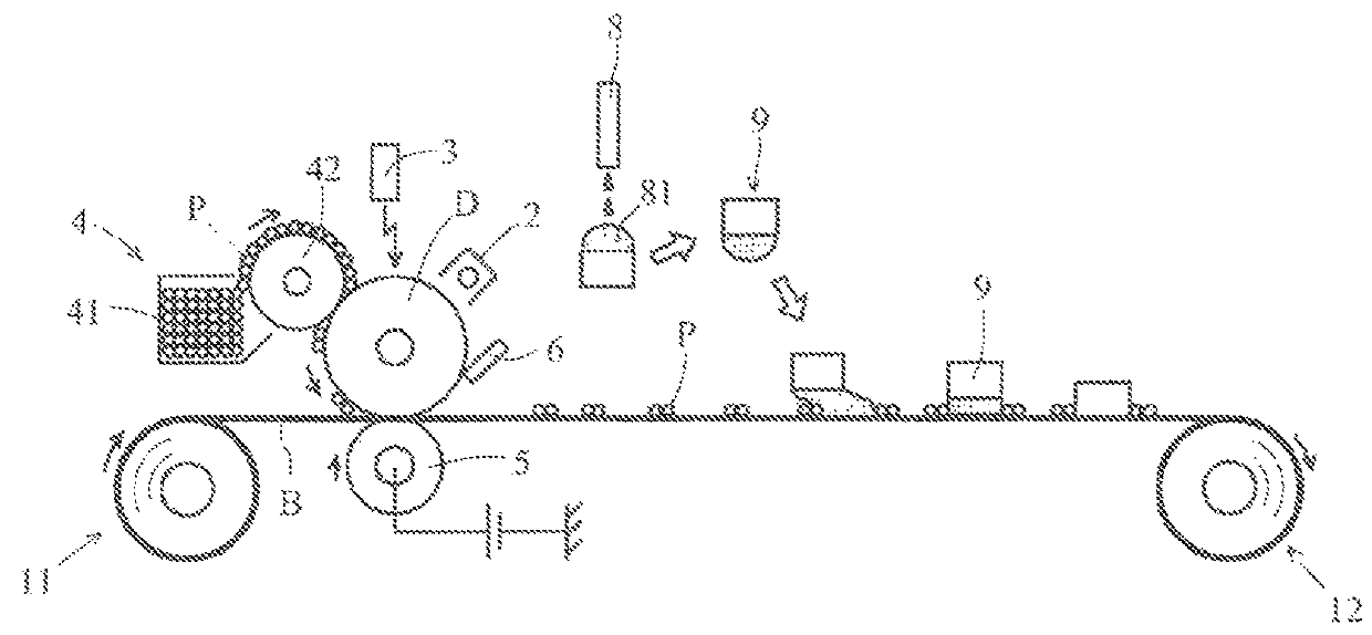
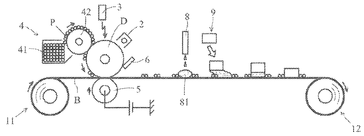
[0046]FIG. 1 is a schematic diagram of a manufacturing device that can continuously perform a method of manufacturing a pattern substrate and a method of locating a component according to the present invention. The device of FIG. 1 includes, around a photoconductive member (particle carrying member) D that is driven to rotate counterclockwise: a charging device 2 that uniformly charges the surface of the photoconductive member D; an exposure device 3 that applies light to the surface of the photoconductive member D to form an electrostatic latent image of a predetermined pattern; a development device 4 that supplies particles (hereinafter, referred to as “liquid-repellent particles”) P which are charged and liquid-repellent to the ph...


PUM

PropertyMeasurementUnit
diameteraaaaaaaaaa
diameteraaaaaaaaaa
particle diameteraaaaaaaaaa

Abstract

There is provided a method of manufacturing a pattern substrate in which a pattern is formed on the surface of the substrate. The manufacturing method includes a step of preparing the substrate and a step of arranging a liquid-repellent or lyophilic material on the surface of the substrate so as to form the pattern on the surface of the substrate in which the surface of the substrate has a liquid-repellent region and a lyophilic region, the pattern is formed by one of the liquid-repellent region and the lyophilic region and the pattern is used to locate a component by the surface tension of a liquid member.

Description

[0001]This application is based on Japanese Patent Application No. 2013-121395 filed on Jun. 10, 2013 the contents of which are hereby incorporated by reference.BACKGROUND OF THE INVENTION[0002]Field of the Invention[0003]The present invention relates to a method of manufacturing a pattern substrate and more particularly relates to, for example, a method of manufacturing a pattern substrate that is used to locate a component utilizing the surface tension of a liquid member.[0004]Description of the Related Art[0005]In recent years, researches on micro-mechanical systems called MEMS (Micro Electro Mechanical Systems) and micro-machines have been widely conducted In order to realize the micro-mechanical system formed with various components described above, it is necessary to provide an assembly system that can achieve mass production.[0006]As a method of arranging a micro-component on a substrate, various types of researches on the autonomous locating of a micro-component are conducte...

Claims


Application Information

Patent Timeline
Patent Type & Authority Patents(United States)
IPC IPC(8): G03G15/20B81C3/00
CPCB81C3/005H01L2224/95146B81C2203/032
Inventor YAMAMOTO, NAOKINAKAYAMA, KANJISAITO, KEITASUWAMA, DAI
Owner KONICA MINOLTA INC
Learn More