Eureka AIR delivers breakthrough ideas for toughest innovation challenges, trusted by R&D personnel around the world.

Touch display panel, method for manufacturing touch display panel, and touch panel display

a technology of touch display panel and touch display panel, which is applied in the direction of solid-state devices, instruments, semiconductor devices, etc., can solve the problems of increasing components cost, reducing yield rate, and needing a lot of manufacturing process and components, so as to reduce the number of components, reduce the effect of visible light transparency and low yield ra

Inactive Publication Date: 2019-04-30
TCL CHINA STAR OPTOELECTRONICS TECH CO LTD
View PDF15 Cites 0 Cited by
  • Summary
  • Abstract
  • Description
  • Claims
  • Application Information

AI Technical Summary

Benefits of technology

[0016]In another aspect of the present invention, the step of patterning the solidified graphene oxide to form the transparent touch electrode layer comprises steps of: patterning the graphene oxide by means of laser shining, and meanwhile, reducing the graphene oxide.
[0020]Compared with conventional technology, a transparent touch electrode with the function of touch is arranged on a display element layer in the display panel in the present invention so that the display panel has the function of touch. Since the display panel has the function of touch, it is unnecessary to add a touch panel on the display panel. Therefore, both of the processes and the number of components are reduced. It is unnecessary to worry about a decrease in visible light transparency because of the touch panel and a low yield rate because of the cohesion of the display panel and the touch panel. To sum up, the touch display panel proposed by the present invention is simplified and optimized with lower production costs.

Problems solved by technology

The drawbacks of the cohesion of the touch panel and the display with the function of touch are as follows: (1) A lot of manufacturing processes and components are needed.
(3) The cohesion of the touch panel and the display panel causes a problem that bubbles easily appear on the interface between the bonded touch panel and display panel when the area of the display screen is large, and accordingly, the touch screen becomes defective, the yield rate decreases, and costs of the components increases.

Method used


Image

  • Touch display panel, method for manufacturing touch display panel, and touch panel display
  • Touch display panel, method for manufacturing touch display panel, and touch panel display
  • Touch display panel, method for manufacturing touch display panel, and touch panel display

Examples


Embodiment Construction

[0031]The accompanying drawings are included to provide a further understanding of the invention, and are incorporated in and constitute a part of this specification. The drawings illustrate embodiments of the invention and, together with the description, serve to explain the principles of the invention.

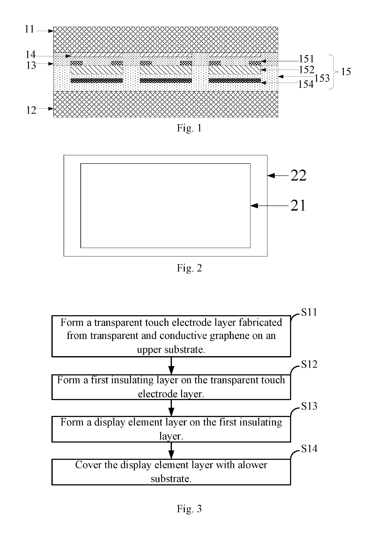
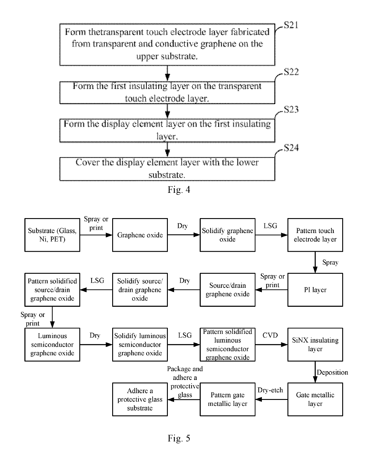
[0032]Please refer to FIG. 1 showing a schematic diagram of the structure of a touch display panel 21 according to one preferred embodiment of the present invention.

[0033]The touch display panel 21 comprises an upper substrate 11, a lower substrate 12, a display element layer arranged between the upper substrate 11 and the lower substrate 12, a first insulating layer 13, and a transparent touch electrode layer 14.

[0034]Preferably, the upper substrate 11 and the lower substrate 12 are fabricated from water- and oxygen-resistant transparent organic material such as polyethylene terephthalate (PET). Otherwise, the upper substrate 11 and the lower substrate 12 are fabricated from glass, ...


PUM


Abstract

The present disclosure proposes a touch display panel, a method for manufacturing touch display panel, and a touch panel display. The touch display panel includes an upper substrate, a lower substrate, a display element layer arranged between the upper substrate and the lower substrate, a first insulating layer, and a transparent touch electrode layer. The display element layer is arranged on the lower substrate for showing images. The first insulating layer is arranged on the display element layer for separating the display element layer from the transparent touch electrode layer. The transparent touch electrode layer is arranged on the first insulating layer for detecting the points where users touch, and the transparent touch electrode layer is fabricated from transparent and conductive graphene. The touch display panel proposed by the present invention is simplified and optimized with lower production costs.

Description

BACKGROUND OF THE INVENTION[0001]1. Field of the Invention[0002]The present invention is related to the field of touch panel display, and more particularly, to a touch display panel, a method for manufacturing the touch display panel, and a touch panel display.[0003]2. Description of the Prior Art[0004]Graphene has features of a solid texture, high transparency (the rate of transmittance ≈97.7%), high heat transfer coefficient (up to 5300 W / m·K), high electron mobility (over 15000 cm2 / V·s). Owing to these features, graphene is increasingly applied to displays, especially in touch screens (replacing transparent conductive thin films, such as indium tin oxide (ITO)) and light-emitting diodes (LED).[0005]A surge of graphene luminous components expands the application of graphene in the field of display. Color of light emitted by LEDs in luminous components fabricated from graphene is adjusted by regulating gate voltage.[0006]A touch panel and a display screen are bonded to form a conve...

Claims


Application Information

Patent Timeline
Patent Type & Authority Patents(United States)
IPC IPC(8): G06F3/041H01L27/32H01L51/00H01L51/50H01L51/10H01L51/05
CPCG06F3/0412G06F3/0416H01L27/32H01L51/0023H01L51/50H01L51/0045H01L51/105G06F2203/04103H01L51/055H10K59/40H10K71/621H10K85/20H10K10/481H10K10/84H10K50/00H10K59/00
Inventor FAN, YONG
Owner TCL CHINA STAR OPTOELECTRONICS TECH CO LTD
Why Eureka
Eureka Blog
Learn More