Efficient memory allocation scheme for data collection

a data collection and memory allocation technology, applied in the field of data storage, can solve the problems of increasing cost and undesirable use of large on-chip memory to store collected statistics, and achieve the effect of reducing asic manufacturing cost and increasing overall hardware efficiency

Inactive Publication Date: 2005-03-17
AVAGO TECH INT SALES PTE LTD
View PDF2 Cites 2 Cited by
  • Summary
  • Abstract
  • Description
  • Claims
  • Application Information

AI Technical Summary

Benefits of technology

[0007] Briefly, the present invention is directed to a system and method that provides an integrated circuit which includes a small on-chip buffer to store collected data, thereby shifting the burden of storing the majority of the collected data to external system memory, which is typically comprised of commodity memory chips. Since this external system memory already exists for use by other system functions, utilizing unused regions of this external memory increases overall hardware efficiency, while achieving lower ASIC manufacturing cost.

Problems solved by technology

This approach of using large on-chip memory to store collected statistics is undesirable because it increases the cost of the ASIC, and does not exploit unused regions of existing system memory.

Method used


Image

  • Efficient memory allocation scheme for data collection
  • Efficient memory allocation scheme for data collection
  • Efficient memory allocation scheme for data collection

Examples


Embodiment Construction

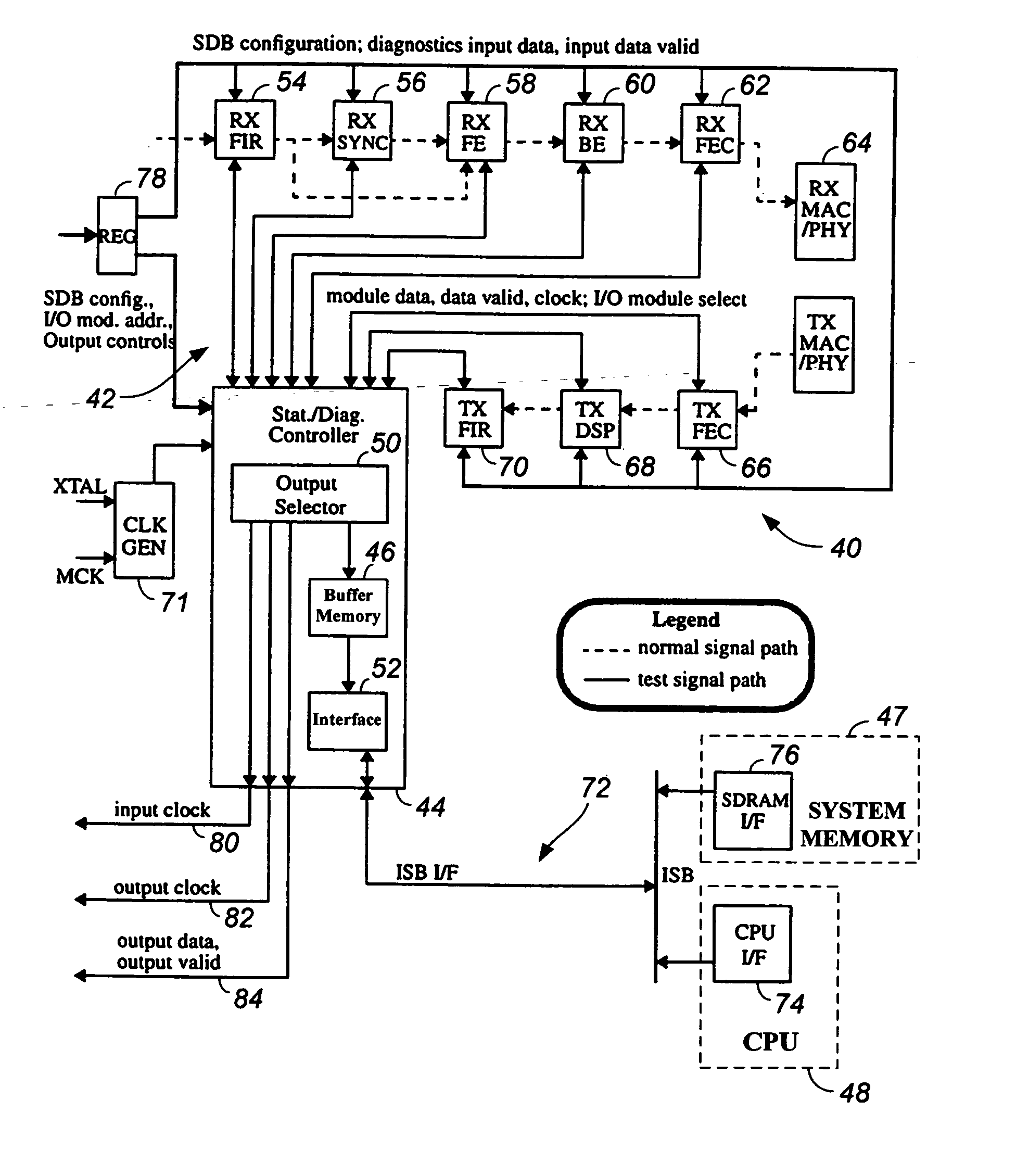
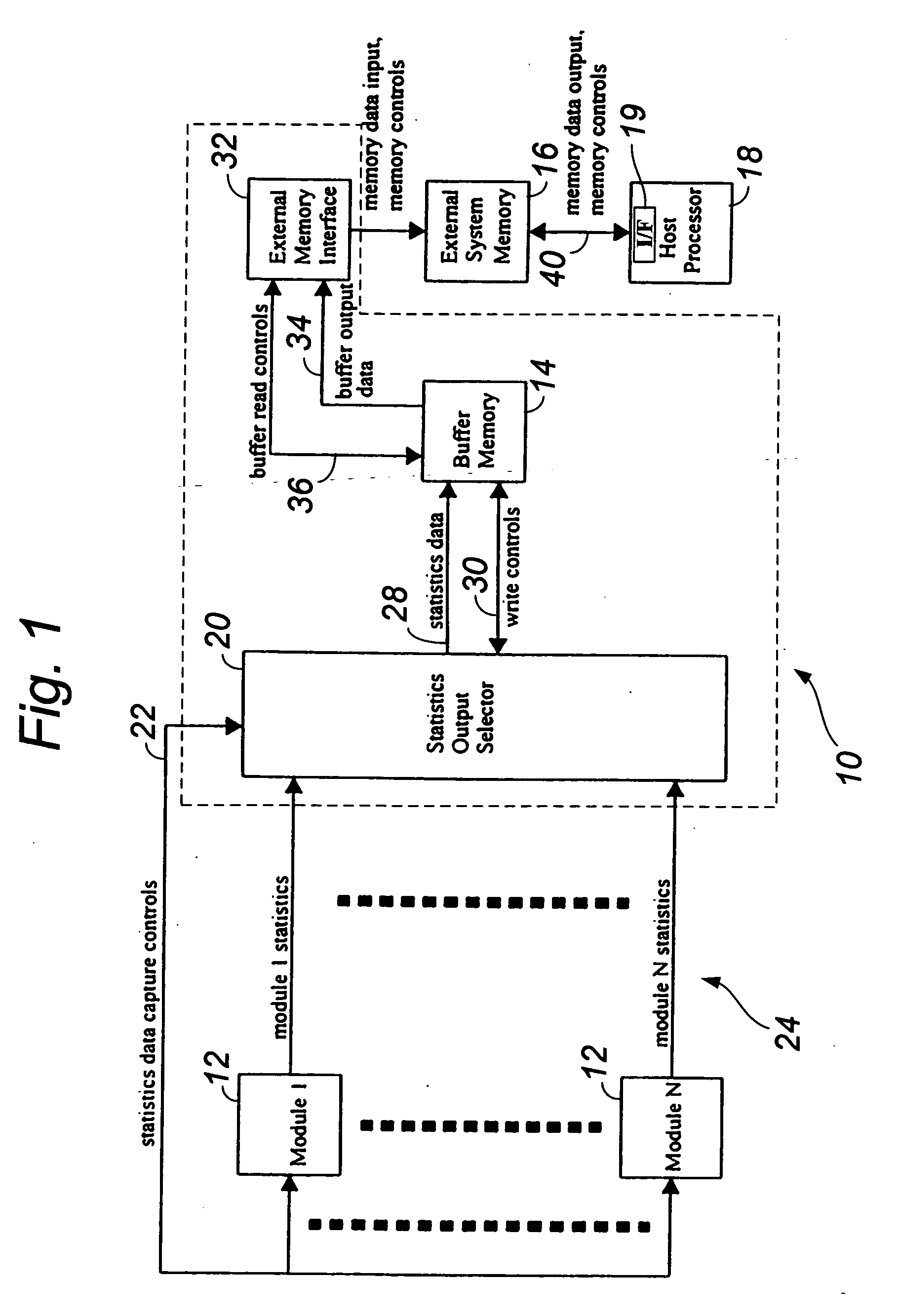
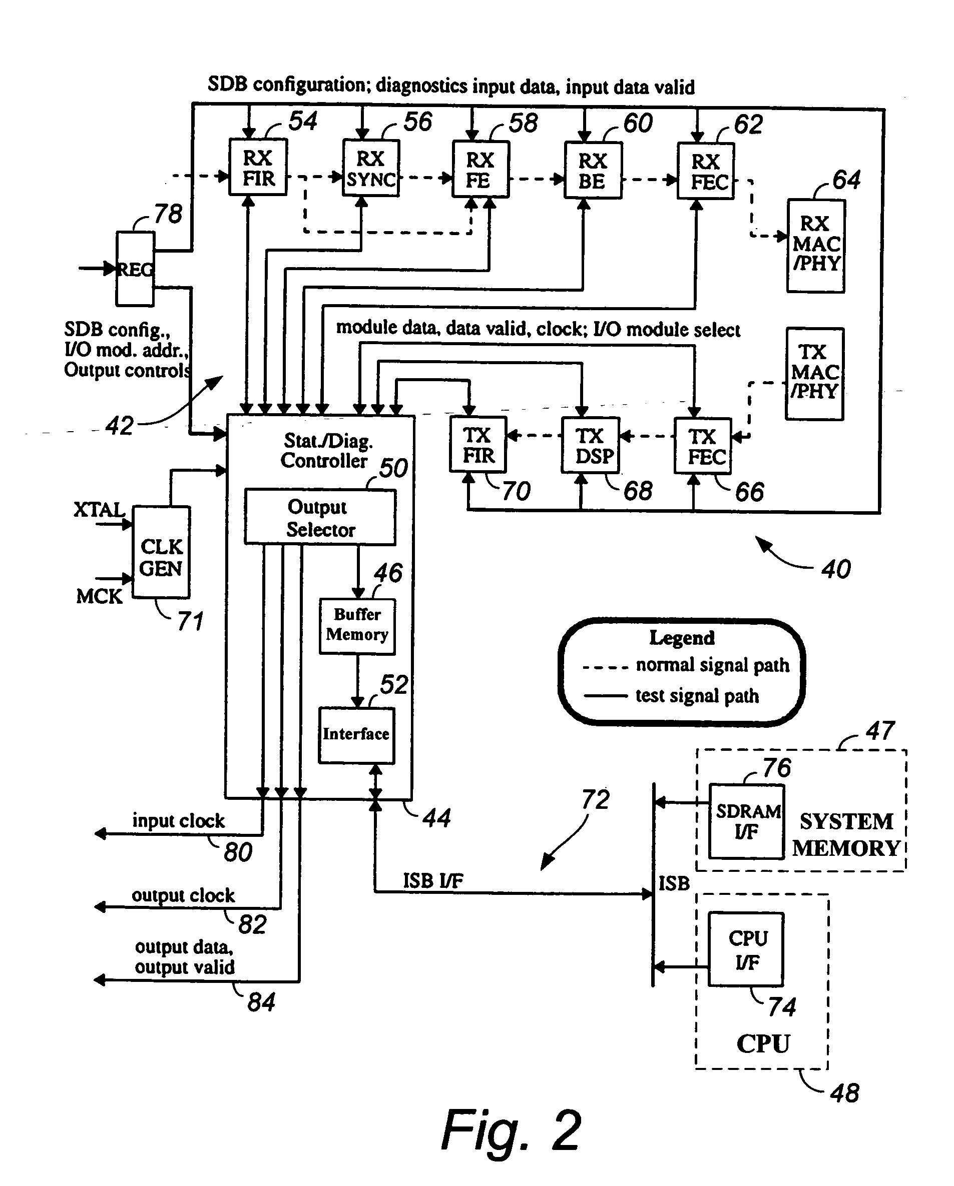
[0013] Referring now to the figures, and in particular to FIG. 1, there is shown one illustrative embodiment of a circuit 10 for collecting and transferring data according to the present invention. Circuit 10 receives data from one or more data collecting and / or generating modules 12, and forwards such data to a buffer memory device 14. Buffer memory device 14 periodically transfers the data to an external system memory 16, which is accessed by a host processor 18 for processing of the collected data, as is described in more detail below.

[0014] In one embodiment, circuit 10 is in the form of an application-specific integrated circuit (ASIC) that is designed to collect data from the module or modules 12. For example, circuit 10 may interact with a plurality of modules 12, where each module monitors a particular system function and generates corresponding data. Such data can correspond to various parameters, such as voltage levels, antenna gain, and the like. Thus, it will be underst...


PUM


Abstract

A system and method that provides an integrated circuit which includes a small on-chip buffer to store collected data, thereby shifting the burden of storing the majority of the collected data to external system memory, which is typically comprised of commodity memory chips. Since this external system memory is already in use by other system functions, utilizing such unused regions of this external memory increases overall hardware efficiency, while achieving lower ASIC manufacturing cost.

Description

CROSS-REFERENCE TO RELATED APPLICATION(S) [0001] This application is a continuation of U.S. patent application Ser. No. 09 / 785,794, filed Feb. 16, 2001, which claims the benefit of the filing date of U.S. Provisional Patent Application No. 60 / 183,615, filed Feb. 18, 2000. The entire content in each of the above-cited applications is incorporated herein by reference.FIELD OF THE INVENTION [0002] The present invention generally relates to the field of data storage. More particularly, the invention relates to an efficient system and method for storing and transferring data within a data-collecting system, such as statistical information collected from monitored functions in communications transceivers. BACKGROUND OF THE INVENTION [0003] Orthogonal Frequency Domain Multiplexing (OFDM) transceiver application-specific integrated circuits (ASIC), such as those used in wireless modems, often include a data collection function that monitors various components of the circuit and collects cor...

Claims


Application Information

Patent Timeline
Patent Type & Authority Applications(United States)
IPC IPC(8): G06F11/34G06F12/00G11C29/00
CPCG06F11/3485G06F11/348
Inventor CHEN, JOEY Y.MOTE, L. RANDALLLIN, THUJI SIMONHEBSGAARD, ANDERS
Owner AVAGO TECH INT SALES PTE LTD
Why Eureka
Try Eureka