
Fabrication method for liquid crystal display
a liquid crystal display and fabrication method technology, applied in the field of fabrication methods for liquid crystal displays, can solve the problems of low orientation and anchoring energy, local exposure to light adversely affecting the orientation after rubbing, etc., and achieve the effect of simple and low-cost fabrication
- Summary
- Abstract
- Description
- Claims
- Application Information
AI Technical Summary
Benefits of technology
Problems solved by technology
Method used
Image

Examples
Embodiment Construction
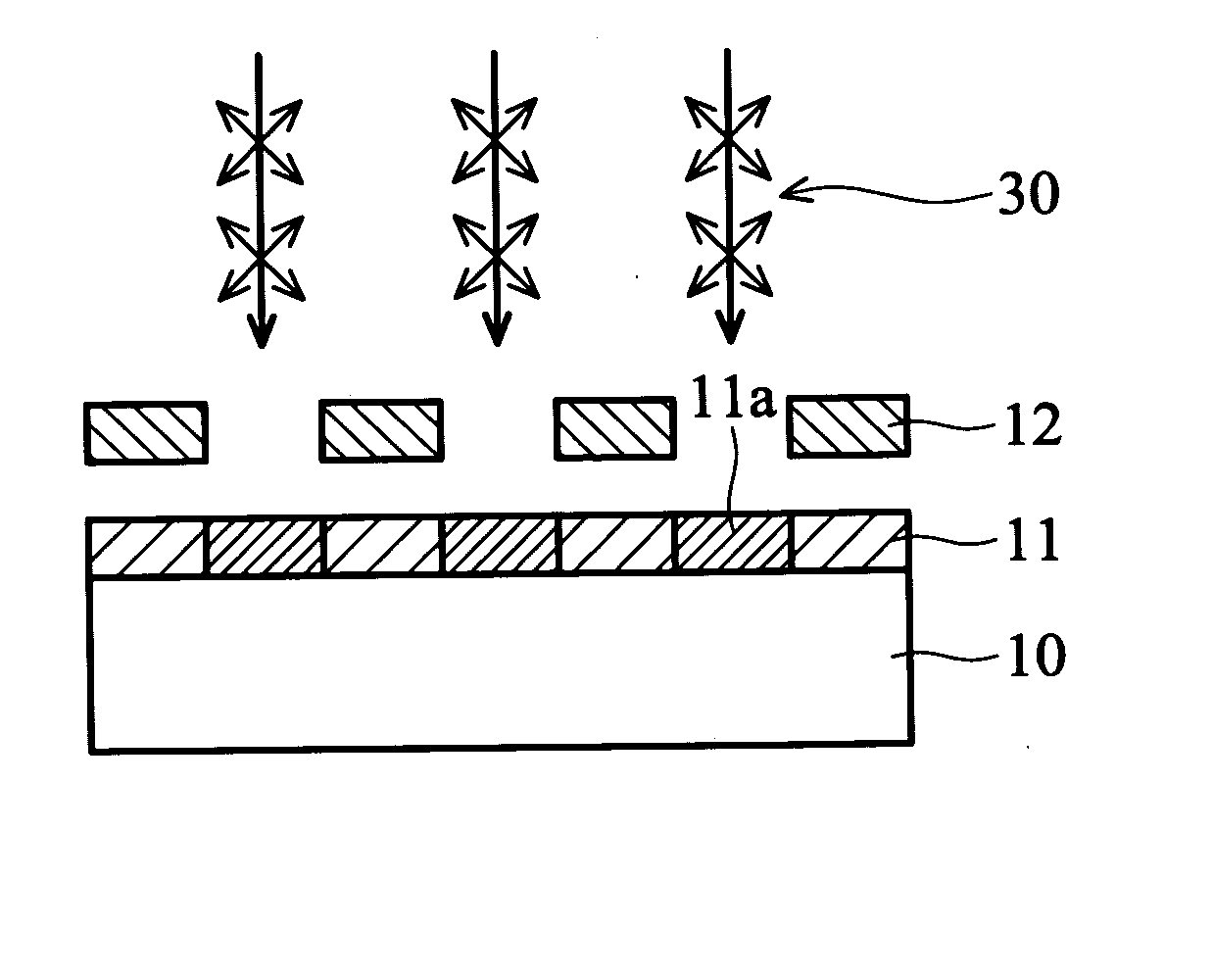
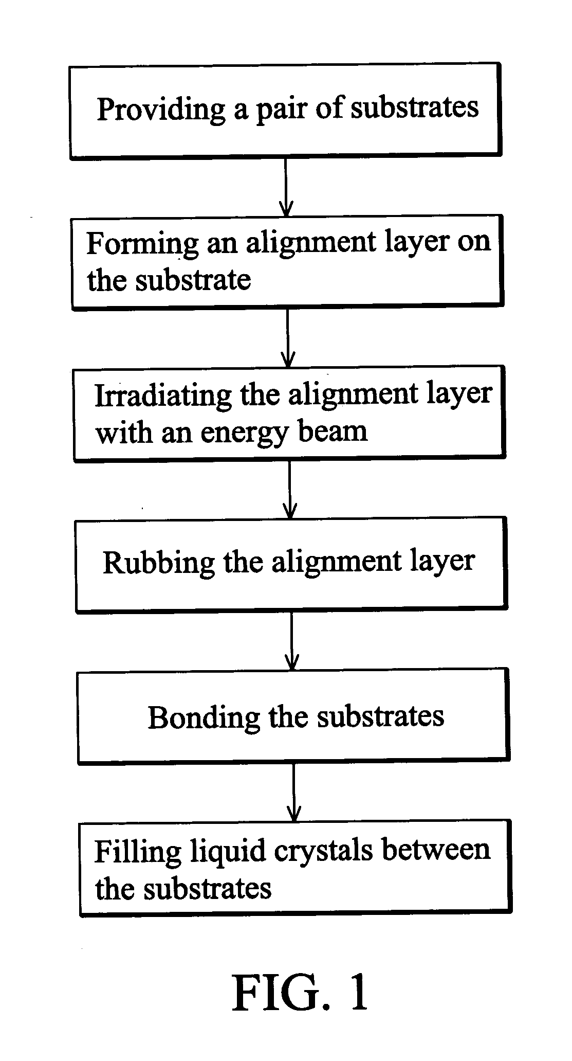
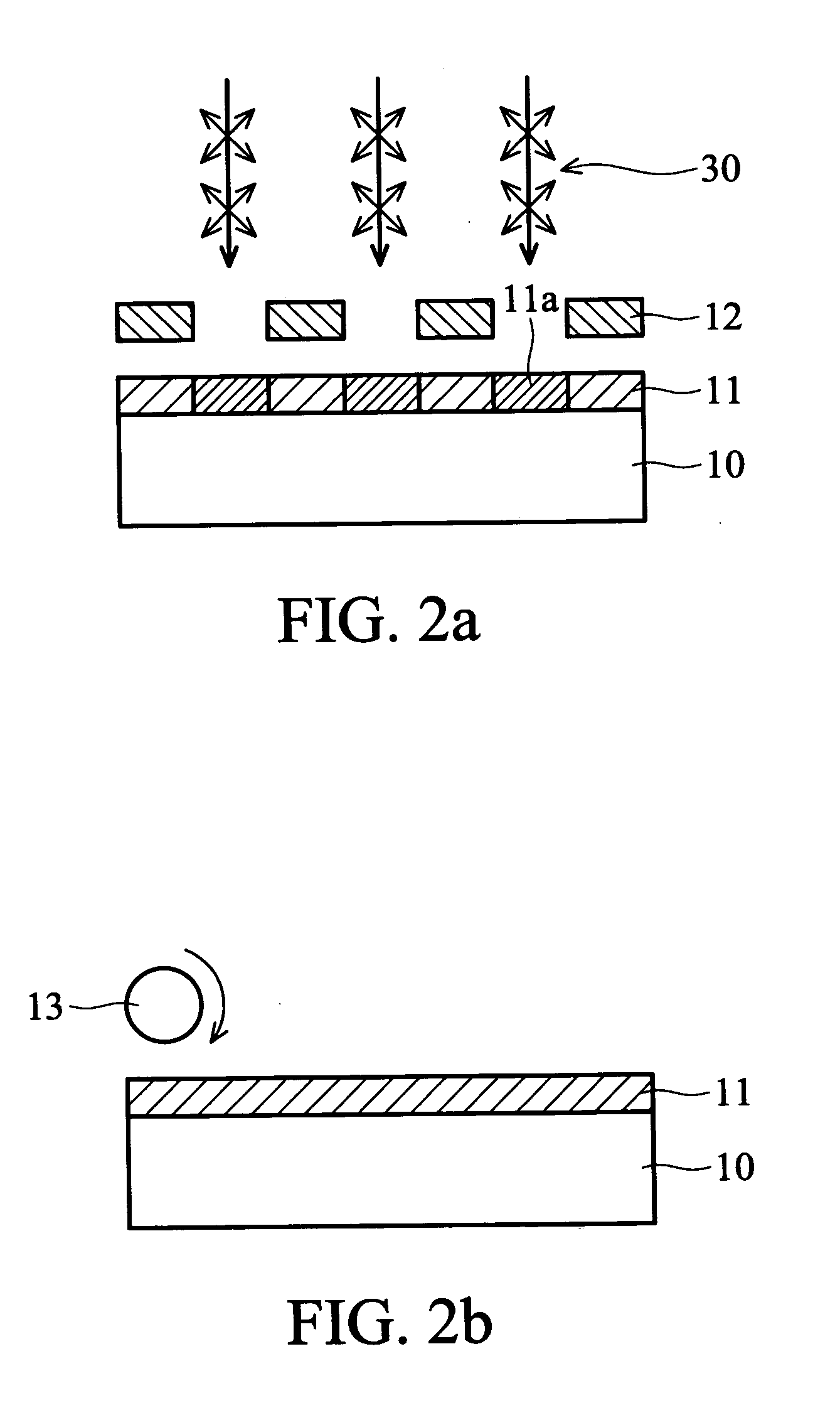
[0021] In the embodiment, a thin film transistor LCD is used as an example to explain the inventive fabrication method. According to the invention, the energy beam exposed on the alignment layer breaks the polymer side chains, and thus may be applied in any form, such as unpolarized electromagnetic wave beam, polarized electromagnetic wave beam, electron beam, laser beam, ion beam or plasma beam. The energy beam may be normally or obliquely incident on the alignment layers.
[0022] First, a pair of substrates 10, 20 (for an LCD panel) is provided. The substrates are, for example, glass or polymeric substrates. Thin film transistors and color filters are manufactured on respective substrates. Next, alignment layers 11, 21 including polyimide, are formed respectively on the substrates 10, 20.
[0023] According to the method, in the case of preparing a vertically aligned alignment layer, the first pretilt angle θ1 is between 0° and the second pretilt angle θ2, in the case of preparing a ...
PUM
| Property | Measurement | Unit |
|---|---|---|
| pretilt angle θ2 | aaaaa | aaaaa |
| pretilt angle θ1 | aaaaa | aaaaa |
| pretilt angle θ1 | aaaaa | aaaaa |
Abstract
Description
Claims
Application Information