Fabrication method for liquid crystal display

a liquid crystal display and fabrication method technology, applied in the field of fabrication methods for liquid crystal displays, can solve the problems of low orientation and anchoring energy, local exposure to light adversely affecting the orientation after rubbing, etc., and achieve the effect of simple and low-cost fabrication

Inactive Publication Date: 2006-06-13
INNOLUX CORP
View PDF5 Cites 8 Cited by
  • Summary
  • Abstract
  • Description
  • Claims
  • Application Information

AI Technical Summary

Benefits of technology

[0011]Accordingly, an object of the present invention is to provide a simple and low-cost fabrication method for an LCD with alignment layers of at least two pretilt-angle areas.
[0015]According to the invention, rubbing is performed after energy-beam exposure. The predetermined area of the alignment layer is exposed to the energy beam, breaking the polymer side chains to thereby reduce the pre-tilt angle of liquid crystals corresponding to the area, and the entire alignment layer is then rubbed with strong anchoring energy, forming a first pretilt angle area in the predetermined area exposed to the energy beam, and a second pretilt angle area in the rest area not exposed to the energy beam. According to the invention, energy-beam exposure is performed before rubbing, such that a linearly polarized energy beam is not required, and undesired effects of exposure on orientation are avoided. The “rubbing after exposure” method ensures overall orientation of alignment.
[0016]Furthermore, in addition to enhancing the orientation and anchoring energy, by utilizing an unpolarized energy beam and / or normal incidence, the equipment required is simplified, thereby reducing costs.

Problems solved by technology

However, photo-alignment requires polarized light in oblique incidence, resulting in low orientation and anchoring energy.
Even though the pretilt angle may be reduced by breaking polymer side chains in the exposure step, owing to the currently limited polarization provided by a polarizing machine (100% polarized light is hard to obtain), local exposure to the light adversely affects the orientation after rubbing.

Method used


Image

  • Fabrication method for liquid crystal display
  • Fabrication method for liquid crystal display
  • Fabrication method for liquid crystal display

Examples


Embodiment Construction

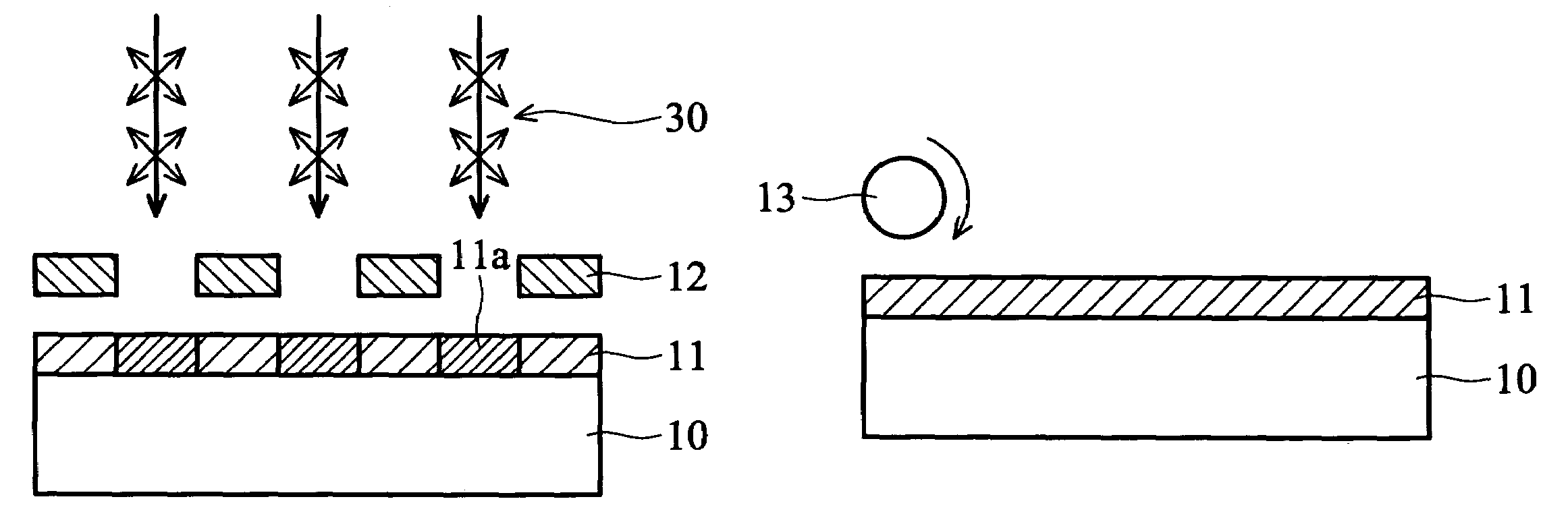
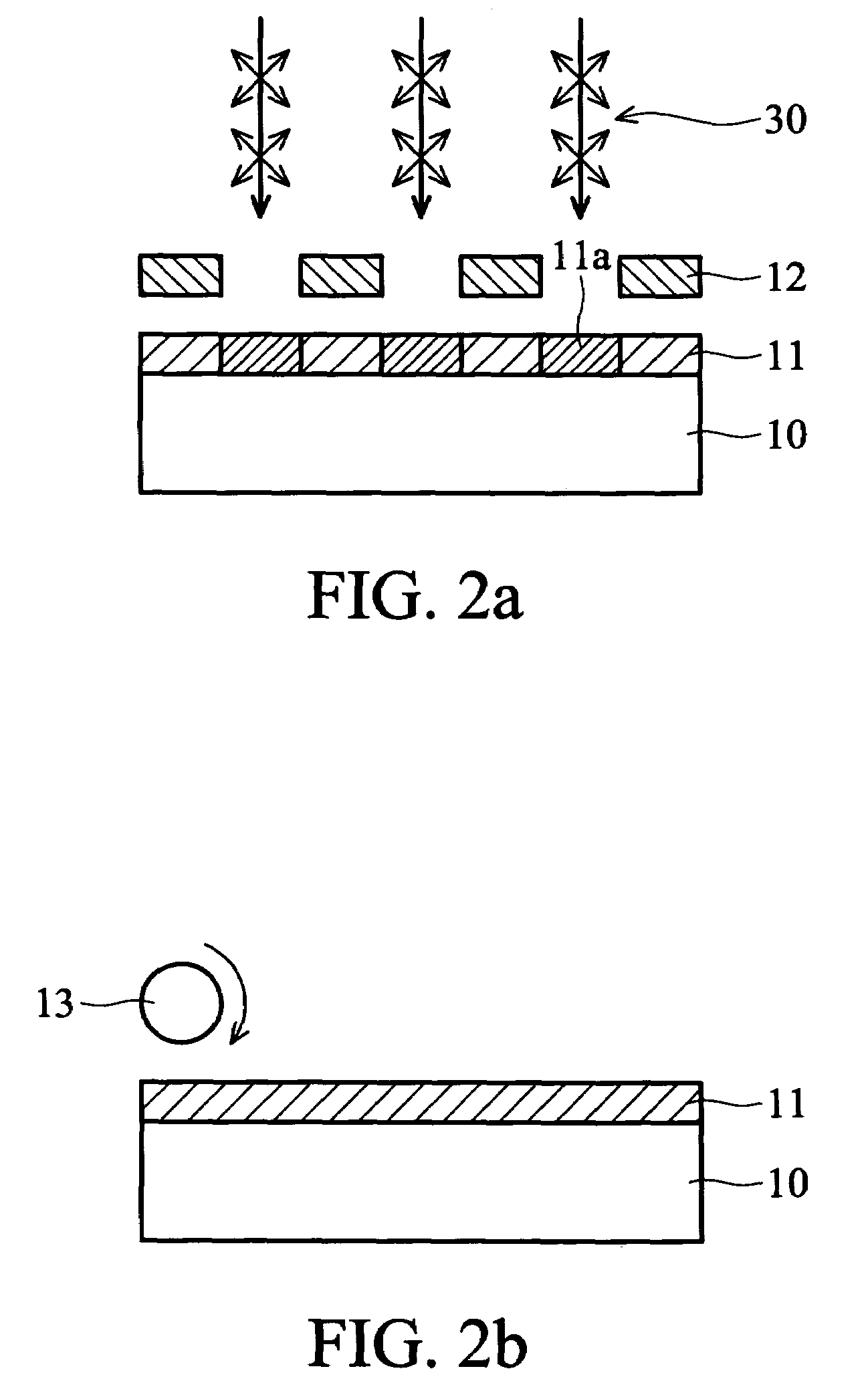
[0023]In the embodiment, a thin film transistor LCD is used as an example to explain the inventive fabrication method. According to the invention, the energy beam exposed on the alignment layer breaks the polymer side chains, and thus may be applied in any form, such as unpolarized electromagnetic wave beam, polarized electromagnetic wave beam, electron beam, laser beam, ion beam or plasma beam. The energy beam may be normally or obliquely incident on the alignment layers.

[0024]First, a pair of substrates 10, 20 (for an LCD panel) is provided. The substrates are, for example, glass or polymeric substrates. Thin film transistors and color filters are manufactured on respective substrates. Next, alignment layers 11, 21 including polyimide, are formed respectively on the substrates 10, 20.

[0025]According to the method, in the case of preparing a vertically aligned alignment layer, the first pretilt angle θ1 is between 0° and the second pretilt angle θ2, in the case of preparing a plana...


PUM

PropertyMeasurementUnit
pretilt angleaaaaaaaaaa
pretilt angle θ1aaaaaaaaaa

Abstract

A fabrication method for a liquid crystal display. A pair of substrates is provided. An alignment layer is formed on the respective substrates. An energy beam is irradiated on a predetermined area of at least one of the alignment layers. The alignment layer is rubbed to form a first pretilt-angle area in the predetermined area exposed to the energy beam, and a second pretilt-angle area not exposed to the energy beam. The pair of substrates are bonded with a preset gap therebetween, and a liquid crystal layer is inserted between the substrates. The liquid crystals corresponding to the first pretilt angle area have a first pretilt angle of θ1, while those corresponding to the second pretilt angle area have a second pretilt angle of θ2.

Description

[0001]This Nonprovisional application claims priority under 35 U.S.C. § 119(a) on Patent Application No(s). 092128058 filed in Taiwan, Republic of China on Oct. 9, 2003, the entire contents of which are hereby incorporated by reference.BACKGROUND OF THE INVENTION[0002]1. Field of the Invention[0003]The present invention relates to a fabrication method for a liquid crystal display, and more particularly to a fabrication method for a liquid crystal display having at least two pretilt angles.[0004]2. Description of the Related Art[0005]Liquid crystal displays (LCD) are commonly used for flat panel display. Owing to dielectric anisotropy and conductive anisotropy of liquid crystal molecules, molecular orientation of liquid crystals can be shifted under an external electronic field, such that various optical effects are produced.[0006]An LCD panel is generally made up of two substrates, with a certain gap preserved therebetween, and a liquid crystal layer filled within the gap. Respectiv...

Claims


Application Information

Patent Timeline
Patent Type & Authority Patents(United States)
IPC IPC(8): G02F1/1337G02F1/13G02F1/1333G02F1/1335G02F1/1368
CPCG02F1/133753G02F1/133784G02F2001/133761G02F1/133761
Inventor FAN, YANG-YICHIANG, HSIN-CHUNLIN, ING JERWONG, YI-CHUNHO, TSAN-YUHSIN, LUNG-PINLIU, KANG-HUNGWU, CHUNG-WENSHA, YI-AN
Owner INNOLUX CORP
Why Eureka
Try Eureka