Semiconductor light emitting device with protrusions to improve external efficiency and crystal growth

a technology of semiconductor devices and protrusions, applied in semiconductor devices, semiconductor/solid-state device details, electrical apparatus, etc., can solve the problems of reducing the efficiency of external quantum energy, reducing so as to reduce the crystallinity of gan, reduce the efficiency of light emission, and facilitate cracking

Active Publication Date: 2010-03-23
NICHIA CORP
View PDF107 Cites 94 Cited by
  • Summary
  • Abstract
  • Description
  • Claims
  • Application Information

AI Technical Summary

Benefits of technology

[0007]However, when a recess or protrusion having insufficient accuracy due to fine structure thereof is formed on a substrate surface without controlling a shape, the recess or protrusion may have significant notches formed on a side face thereof, resulting in a rugged circumference (FIG. 14). A GaN layer grown on such a substrate surface is likely to have pits and / or voids, which in turn make it easier for cracks to occur during regrowth of GaN. This results in lower crystallinity of GaN which decreases efficiency of light emission (internal quantum efficiency), and thus external quantum efficiency decreases contrary to an intention. These cracks also lower reliability of this semiconductor device. Influence of lowering crystallinity of the semiconductor is not limited to a light emitting device such as a light emitting diode, but adversely affects other semiconductor devices such as a light sensor and electronic devices.
[0008]When a recess or protrusion is formed on a substrate surface whereon a semiconductor is to be grown, the semiconductor may grow with anomaly that may result in various problems. For example, such problems may result as deterioration of surface morphology caused by pits formed in a semiconductor layer surface and the like; occurrence of voids caused by insufficient semiconductor growth without filling the recess; threading dislocation and other crystalline defects caused in the semiconductor layer by defective growth of the semiconductor; or occurrence of a partial abnormal growth in a wafer surface. Undesirable surface morphology due to pits or other like structure formed in the surface, or poor crystallinity due to crystal defects, lead to an increase in electrostatic discharge damage due to leakage current, or decreased efficiency of light emission due to subsequently deteriorated crystallinity of an active layer or the like, which may result in unsatisfactory properties of a semiconductor device. Voids caused by the recess or protrusion may cause poor crystallinity and / or pits and may also hamper an optical effect of the recess or protrusion in the substrate. When a partial abnormal growth occurs in a wafer, a lower yield of device production results.
[0009]In consideration of the problems described above, an object of the present invention is to provide a semiconductor device characterized by high reliability including electrostatic discharge tolerance, better crystallinity and high efficiency of light emission, by suppressing generation of pits and voids in a semiconductor layer due to formation of a recess or protrusion on a substrate surface. Another object of the present invention is to provide a semiconductor device that can be manufactured with a high yield of production while achieving stable external quantum efficiency, and a method of manufacturing the same.

Problems solved by technology

However, when a recess or protrusion having insufficient accuracy due to fine structure thereof is formed on a substrate surface without controlling a shape, the recess or protrusion may have significant notches formed on a side face thereof, resulting in a rugged circumference (FIG. 14).
This results in lower crystallinity of GaN which decreases efficiency of light emission (internal quantum efficiency), and thus external quantum efficiency decreases contrary to an intention.
These cracks also lower reliability of this semiconductor device.
Influence of lowering crystallinity of the semiconductor is not limited to a light emitting device such as a light emitting diode, but adversely affects other semiconductor devices such as a light sensor and electronic devices.
When a recess or protrusion is formed on a substrate surface whereon a semiconductor is to be grown, the semiconductor may grow with anomaly that may result in various problems.
For example, such problems may result as deterioration of surface morphology caused by pits formed in a semiconductor layer surface and the like; occurrence of voids caused by insufficient semiconductor growth without filling the recess; threading dislocation and other crystalline defects caused in the semiconductor layer by defective growth of the semiconductor; or occurrence of a partial abnormal growth in a wafer surface.
Undesirable surface morphology due to pits or other like structure formed in the surface, or poor crystallinity due to crystal defects, lead to an increase in electrostatic discharge damage due to leakage current, or decreased efficiency of light emission due to subsequently deteriorated crystallinity of an active layer or the like, which may result in unsatisfactory properties of a semiconductor device.
Voids caused by the recess or protrusion may cause poor crystallinity and / or pits and may also hamper an optical effect of the recess or protrusion in the substrate.
When a partial abnormal growth occurs in a wafer, a lower yield of device production results.

Method used


Image

  • Semiconductor light emitting device with protrusions to improve external efficiency and crystal growth
  • Semiconductor light emitting device with protrusions to improve external efficiency and crystal growth
  • Semiconductor light emitting device with protrusions to improve external efficiency and crystal growth

Examples


embodiment 1

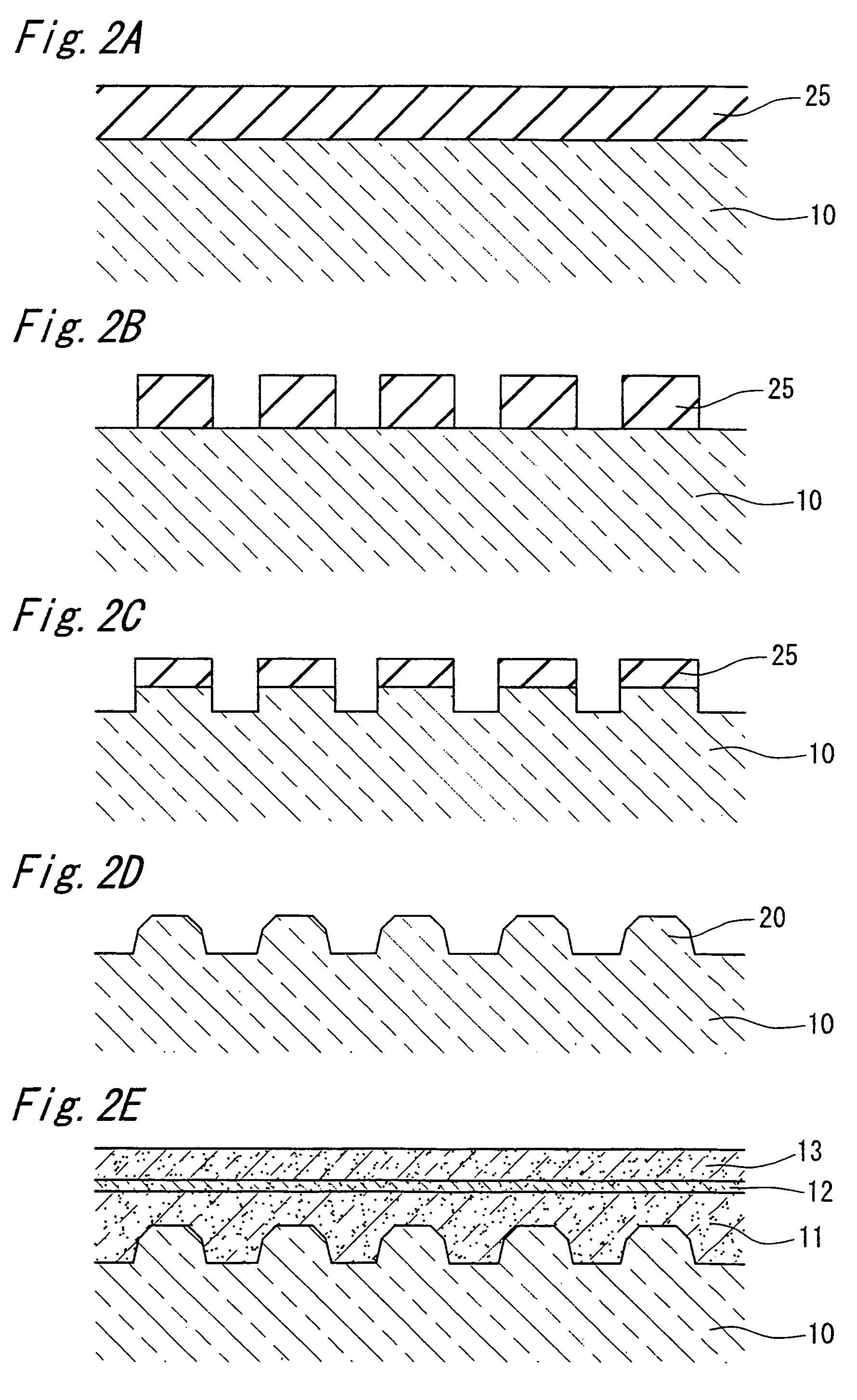
[0109]In a first embodiment of the present invention, the side face of the protrusion consists of at least two sloped surfaces (first sloped surface 22, second sloped surface 23) as shown in FIG. 4A and FIG. 5A. An inclination angle θ2 on a top face side of the protrusion is smaller than an inclination angle θ1 on a bottom side. The inclination angle θ is an angle between the side face and a bottom of the protrusion. In case recesses are formed in the substrate, an inner wall of each recess is also formed so that the inclination angle θ2 of an upper inner wall is larger than an inclination angle θ1 of a lower inner wall. The inclination angle θ1 of the inner wall is a complementary angle of angle Φi between the inner wall and a bottom surface of the recess.

θi=180°−Φi (i=1, 2)

When inclination angle θ3 is defined as an angle between the top face and the side face of the protrusion, in case the top face is substantially parallel to the substrate surface, angle Φ2 between the upper inne...

embodiment 2

[0110]In a second embodiment of the invention, a side face of the protrusion is formed as a curved surface. In case an entire side face of the protrusion is formed of a single curved surface, a radius of curvature may be made larger on a top face side and smaller on a bottom side.

[0111]Alternatively, such a configuration may also be employed as the bottom side being flat, i.e., an upper side of the side face is curved and the lower side is flat. Moreover, a plurality of curved portions and a plurality of flat portions may be formed on the side face of the protrusion. For example, in a structure of the first embodiment where the first and second sloped surfaces are formed, the second sloped surface may be formed as a curved surface with the first sloped surface consisting of a substantially flat surface. A condition of the side face may be selected as required in accordance with substrate material, an etching condition, material of a semiconductor layer and other factors.

[0112]It is ...

embodiment 3

Structure of Light Emitting Device

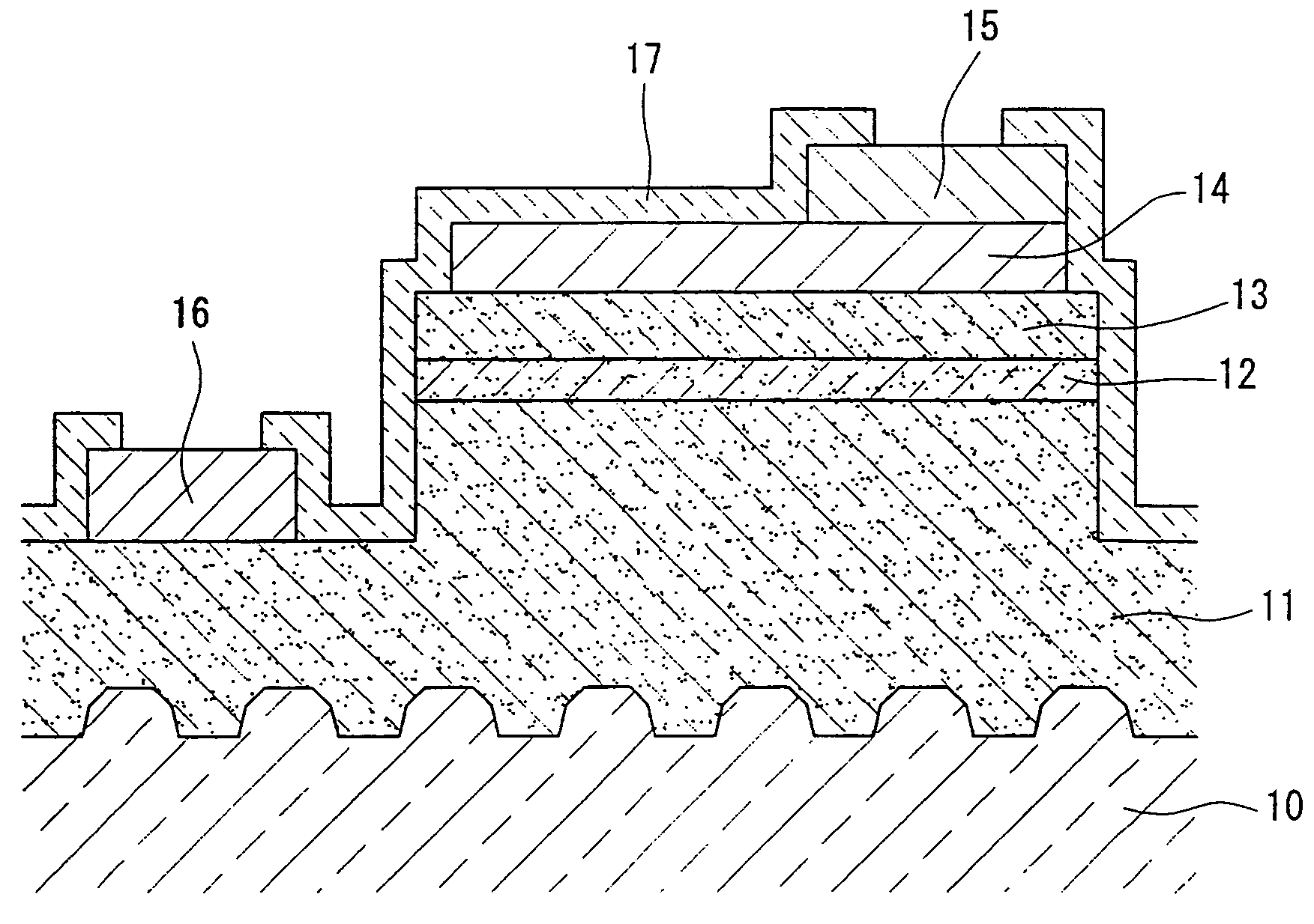
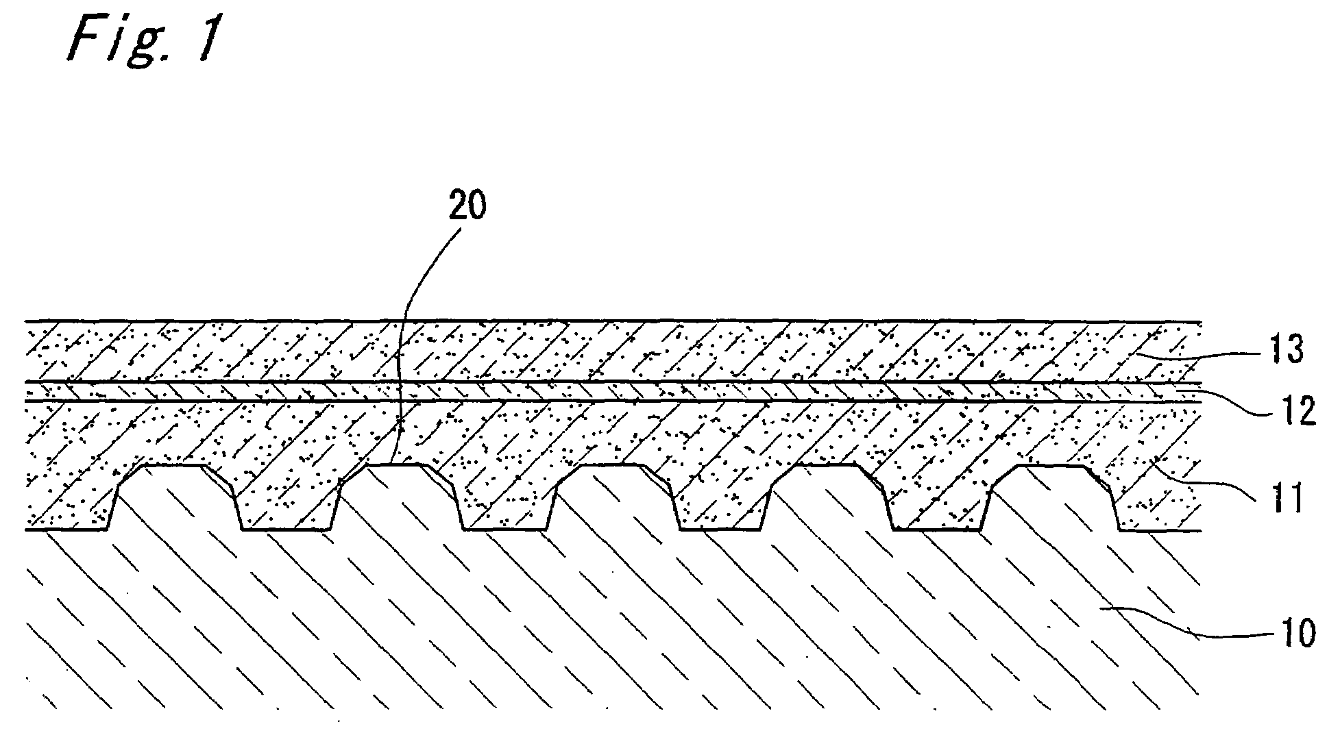
[0113]Constitution of a semiconductor light emitting device according to the present invention will be described in detail. There are no specific requirements for a size and thickness of the substrate 10 which may be of any constitution as long as it allows epitaxial growth of a semiconductor thereon. The substrate used to grow a nitride semiconductor thereon may be made of an insulating material such as sapphire or spinel (MgAl2O4) having a principal plane as a C plane, R plane or A plane, or an oxide such as lithium niobate or neodymium gallate that forms a lattice junction with silicon carbide (6H, 4H, 3C), silicon, ZnS, ZnO, Si, GaAs, diamond, or oxide substrates such as lithium niobate or neodymium gallate, which can provide a good lattice match with a nitride semiconductor. A substrate made of a nitride semiconductor such as GaN or AlN may also be used provided that it is thick enough to form devices thereon (over several tens of micrometers)....


PUM


Abstract

A substrate has at least one recess and / or protrusion formed in and / or on a surface thereof so as to scatter or diffract light generated in an active layer. The recess and / or protrusion is formed in such a shape that can reduce crystalline defects in semiconductor layers.

Description

TECHNICAL FIELD[0001]The present invention relates to a semiconductor device having a recess or protrusion provided on a substrate and, more particularly, to a semiconductor light emitting device that improves its external efficiency by having the recess or protrusion provided on the substrate.BACKGROUND ART[0002]A semiconductor device, for example, a light emitting diode (LED) essentially comprises an n-type semiconductor layer, an active layer and a p-type semiconductor layer laminated on a substrate in this order. Electrodes are formed on the p-type semiconductor layer and on the n-type semiconductor layer. Light is generated in a light emitting region of the active layer through recombination of holes injected from the p-type semiconductor layer and electrons injected from the n-type semiconductor layer. The light is extracted to outside from a surface whereon the electrodes are formed, or from a back surface of the substrate where a semiconductor layer is not formed.[0003]A lig...

Claims


Application Information

Patent Timeline
Patent Type & Authority Patents(United States)
IPC IPC(8): H01L29/18H01L21/3065H01L21/48H01L33/06H01L23/04H01L33/00H01L33/22H01L33/24H01L33/32H01L33/38H01L33/40H01L33/62
CPCH01L21/0237H01L21/0242H01L21/0243H01L21/02433H01L21/0254H01L21/02658H01L33/007H01L33/20H01L2924/3025H01L2224/49107H01L2224/48465H01L2224/48247H01L21/02647H01L25/167H01L33/22H01L33/38H01L2933/0083H01L2924/00H01L2924/181H01L2224/48095H01L2924/13091H01L2924/00012
Inventor TANAKA, HISANORIHOSOKAWA, YASUNOBUSHIBUTANI, YUUKI
Owner NICHIA CORP
Why Eureka
Try Eureka