GaN Substrate, Substrate with an Epitaxial Layer, Semiconductor Device, and GaN Substrate Manufacturing Method

a technology of epitaxial layer and substrate, applied in the direction of manufacturing tools, natural mineral layered products, crystal growth process, etc., can solve the problem of low emission efficiency of emission-wavelength, and achieve the effect of enhancing emission efficiency, stably manufacturing, and enhancing emission efficiency

Inactive Publication Date: 2008-12-18
SUMITOMO ELECTRIC IND LTD
View PDF5 Cites 234 Cited by
  • Summary
  • Abstract
  • Description
  • Claims
  • Application Information

AI Technical Summary

Benefits of technology

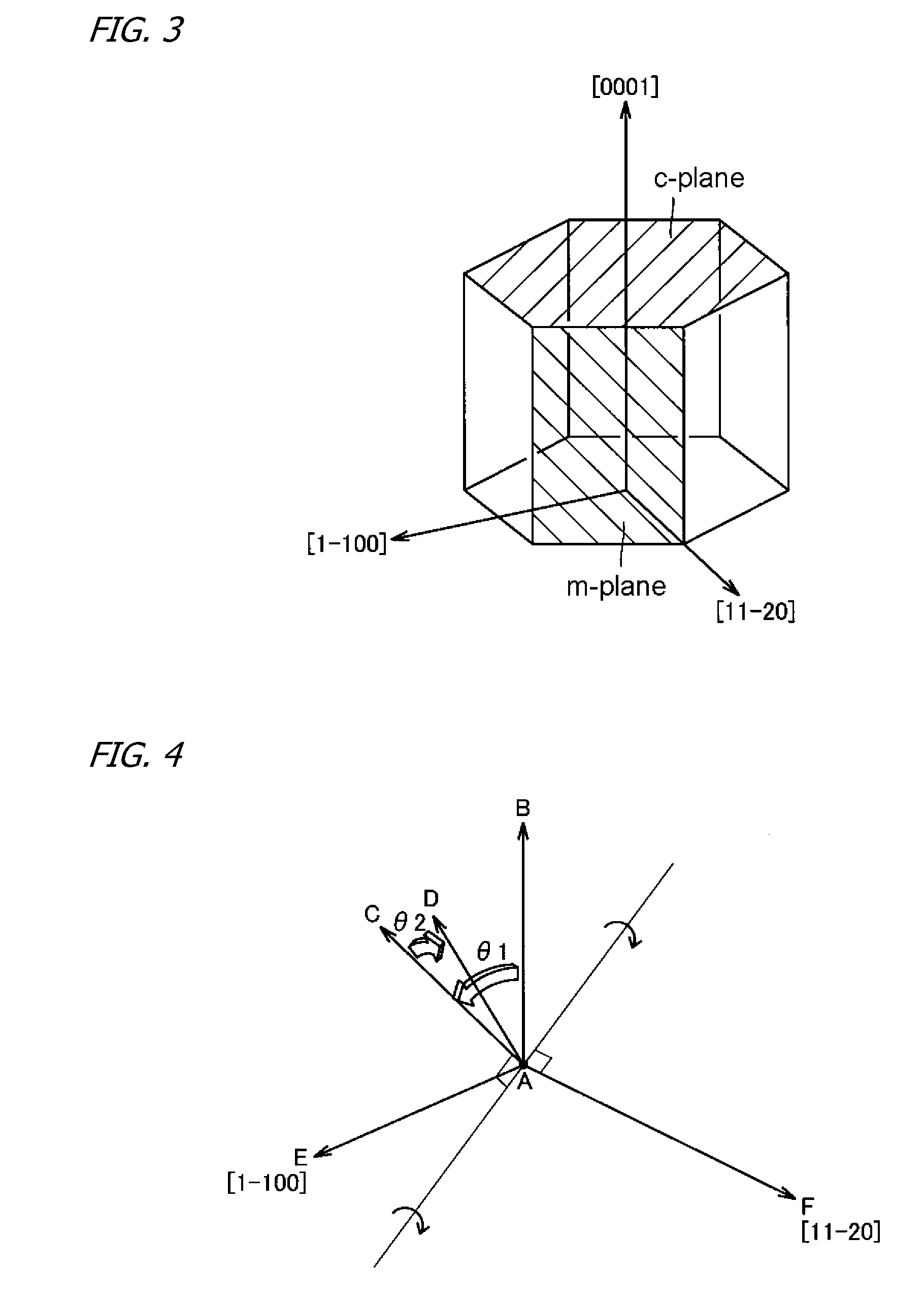
[0008]With the above-described GaN substrate manufacturing method disclosed in Japanese Unexamined Pat. App. Pub. No. 2005-298319, the inventors of the present invention prepared GaN substrates having different off-axis angles, and formed an epitaxial layer on the GaN substrate principal surfaces to experimentally produce LEDs. As a result of examining their properties, the inventors found that with respect to a normal to the principal surface of a GaN substrate, inclining the [0001] plane orientation in one plane orientation (one off-axis direction) makes the crystal plane exposed on the GaN substrate surface semipolar, and further inclining the [0001] plane orientation in a different plane orientation (in a different off-axis direction) enables controlling (decreasing) fluctuations in the wavelength distribution along the GaN substrate principal surface. More precisely, a GaN substrate in one aspect of the present invention is a GaN substrate having a principal surface with respect to whose normal vector the [0001] plane orientation is inclined in two different off-axis directions.
[0009]Such a GaN substrate permits, with the substrate principal surface being made semipolar by inclining the [0001] plane orientation in a first off-axis direction, epitaxial layer formation on the principal surface. Therefore, forming an epitaxial layer on the principal surface that has been made semipolar heightens the emission efficiency of a light-emitting device whose emission wavelengths are included in a longer-wavelength range of 500 nm or more, and makes the amount of wavelength shift caused by variation of the amount of applied electric current smaller, than forming an epitaxial layer on a GaN substrate polar surface such as the (0001) plane to manufacture LEDs and other light-emitting devices. Additionally, further inclining the [0001] plane orientation in a second off-angle direction enables controlling in-plane wavelength fluctuations in the GaN substrate principal surface. As a result, by employing such GaN substrates, superiorly performing LEDs and like semiconductor devices can be manufactured stably.
[0010]The substrate with an epitaxial layer in another aspect of the present invention is provided with the GaN substrate and an epitaxially grown layer formed on the GaN substrate principal surface. Forming the epitaxially grown layer on the GaN substrate principal surface means that the epitaxially grown layer is formed on the semipolar surface of the GaN substrate, making it possible to afford the substrate with an epitaxial layer from which semiconductor devices such as light-emitting devices whose emission wavelengths are included in a range of long wavelength of 500 nm or more, and whose emission efficiencies have been enhanced can be stably manufactured.
[0011]In the semiconductor device in a further aspect of the present invention, the substrate with an epitaxial layer is employed. Employing this substrate with an epitaxial layer enables obtaining semiconductor devices such as light-emitting devices whose emission wavelengths are included in a longer-wavelength range of 500 nm or more, and whose emission efficiencies are enhanced, with a little amount of wavelength shift in accordance with the amount of applied electric current.
[0012]The GaN substrate manufacturing method in yet another aspect of the present invention is provided with the following steps. That is, first, a step of preparing an undersubstrate with respect to whose principal surface normal vector a reference or fiducial plane is inclined in two different inclination directions toward the undersubstrate is carried out. A step of growing a GaN crystal layer on the undersubstrate principal surface is performed. A step of removing the undersubstrate from the GaN crystal layer to produce a GaN substrate composed of the GaN crystal layer is carried out. The GaN substrate has a principal surface, with [0001] plane orientation inclining in two different off-axis angles with respect to the substrate principal surface normal vector. Changing the angles at which the undersubstrate fiducial plane orientation is inclined in the inclination directions toward undersubstrate adjusts the angles at which the GaN substrate [0001] plane orientation is inclined in the off-axis angles. As a result, the GaN substrate of the present invention can be readily produced. Also, such a change of the angles at which the undersubstrate fiducial orientation is inclined in the inclination directions toward undersubstrate facilitates manufacturing of the GaN substrate in which the inclination angles in the off-axis directions are varied to any angles.

Problems solved by technology

A problem with thus-formed LDs and LEDs has been that because the (0001) plane of the GaN or other substrate is the polar plane, the LED emission efficiency drops for emission-wavelength ranges of wavelengths longer than 500 nm.

Method used


Image

  • GaN Substrate, Substrate with an Epitaxial Layer, Semiconductor Device, and GaN Substrate Manufacturing Method
  • GaN Substrate, Substrate with an Epitaxial Layer, Semiconductor Device, and GaN Substrate Manufacturing Method
  • GaN Substrate, Substrate with an Epitaxial Layer, Semiconductor Device, and GaN Substrate Manufacturing Method

Examples


embodiment 1

[0067]Next, in order to confirm the effects of the present invention, the following experiment was carried out. Namely, a GaN substrate in accordance with the present invention was prepared, and a light-emitting device utilizing the GaN substrate was produced. Subsequently, as to the GaN substrate and light-emitting device, the relationship between the wavelength of emitted light and the amount of supplied electric current was measured, as will be described hereinafter. Furthermore, for comparison, the first GaN substrate whose principal surface was rendered c-plane, and the second GaN substrate whose principal surface was rendered m-plane were prepared, and light-emitting devices as comparative examples were formed employing these GaN substrates. Subsequently, as to these comparative light-emitting devices, the properties similar to those of the first and second GaN substrates were measured. The experiment will be described in detail hereinafter.

1. Preparation of GaN Substrate

1-1. ...

embodiment 2

[0091]In order to confirm the effectiveness of the present invention, the following experiment was carried out. Specifically, GaN substrates: test sample ID Nos. 1 to 70 were prepared, and as to these GaN substrate test samples, off-axis directions, off-axis angles, and furthermore, off-axis angle in-plane distribution, and dislocation density were measured. Moreover, light-emitting devices were formed employing the GaN substrates to measure the amount of emission wavelength change (blue shift: Δλ) caused by varying the electric current applied to the light-emitting devices, the amount of increase in operating voltage (ΔVop) when 1000 hours passed, and emission wavelength distribution (σ) in the GaN substrate surface. Below, the experiment will be described in detail.

1. GaN Substrate Preparation

[0092]As to all the test samples (test sample ID Nos. 1 to 70), GaN substrates were prepared by employing the basically same manner as in Embodiment 1 described above.

[0093]Undersubstrate:

[00...


PUM

PropertyMeasurementUnit
anglesaaaaaaaaaa
anglesaaaaaaaaaa
wavelengthsaaaaaaaaaa

Abstract

Affords a GaN substrate from which enhanced-emission-efficiency light-emitting and like semiconductor devices can be produced, an epi-substrate in which an epitaxial layer has been formed on the GaN substrate principal surface, a semiconductor device, and a method of manufacturing the GaN substrate. The GaN substrate is a substrate having a principal surface with respect to whose normal vector the [0001] plane orientation is inclined in two different off-axis directions.

Description

BACKGROUND OF THE INVENTION[0001]1. Technical Field[0002]The present invention relates to GaN substrates, to substrates with an epitaxial layer, to semiconductor devices, and to methods of manufacturing GaN substrates, and more specifically relates to GaN substrates having utilizable semipolar surfaces, to such substrates and semiconductor devices with an epitaxial layer, and to methods of manufacturing such GaN substrates.[0003]2. Description of the Related Art[0004]Conventionally, GaN laser diodes (LD) and light-emitting diodes (LED) are well known. GaN LDs and LEDs have been formed by depositing epitaxial layers onto the (0001) surface of a sapphire, SiC or GaN substrate. A problem with thus-formed LDs and LEDs has been that because the (0001) plane of the GaN or other substrate is the polar plane, the LED emission efficiency drops for emission-wavelength ranges of wavelengths longer than 500 nm.[0005]“Press Release: Success in Developing LEDs on Semipolar Bulk GaN Substrates,” [...

Claims


Application Information

Patent Timeline
Patent Type & Authority Applications(United States)
IPC IPC(8): H01L29/20B23B9/00H01L21/205
CPCH01L21/02433H01L21/0254H01L21/02639C23C16/01C23C16/303C30B25/02C30B25/04C30B25/18C30B29/406H01L21/02378H01L21/02389H01L21/02395H01L21/02403H01L21/0242
Inventor KASAI, HITOSHIISHIBASHI, KEIJINAKAHATA, SEIJIAKITA, KATSUSHIKYONO, TAKASHIMIURA, YOSHIKI
Owner SUMITOMO ELECTRIC IND LTD
Why Eureka
Try Eureka