Anti-stiction technique for thin film and wafer-bonded encapsulated microelectromechanical systems

US20050095833A1Active Publication Date: 2005-05-05ROBERT BOSCH GMBH

Image

  • Anti-stiction technique for thin film and wafer-bonded encapsulated microelectromechanical systems
  • Anti-stiction technique for thin film and wafer-bonded encapsulated microelectromechanical systems
  • Anti-stiction technique for thin film and wafer-bonded encapsulated microelectromechanical systems

Examples


Embodiment Construction

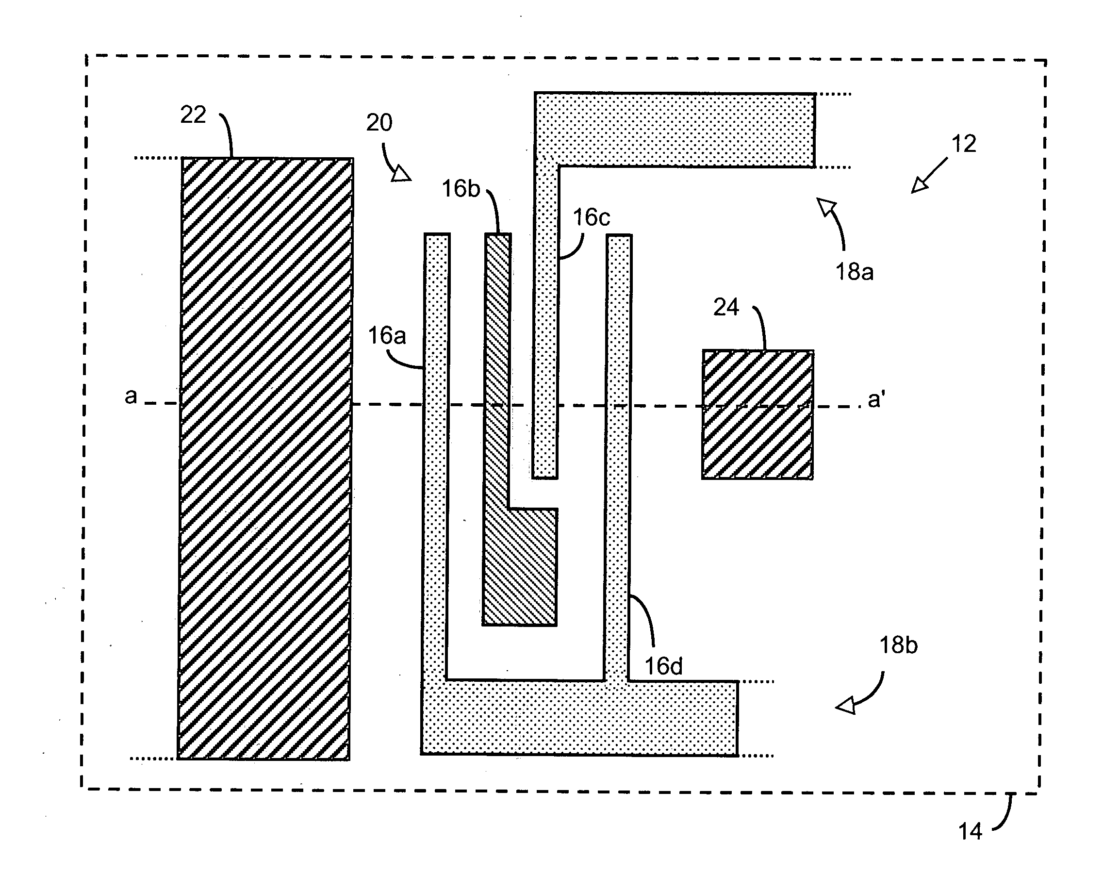
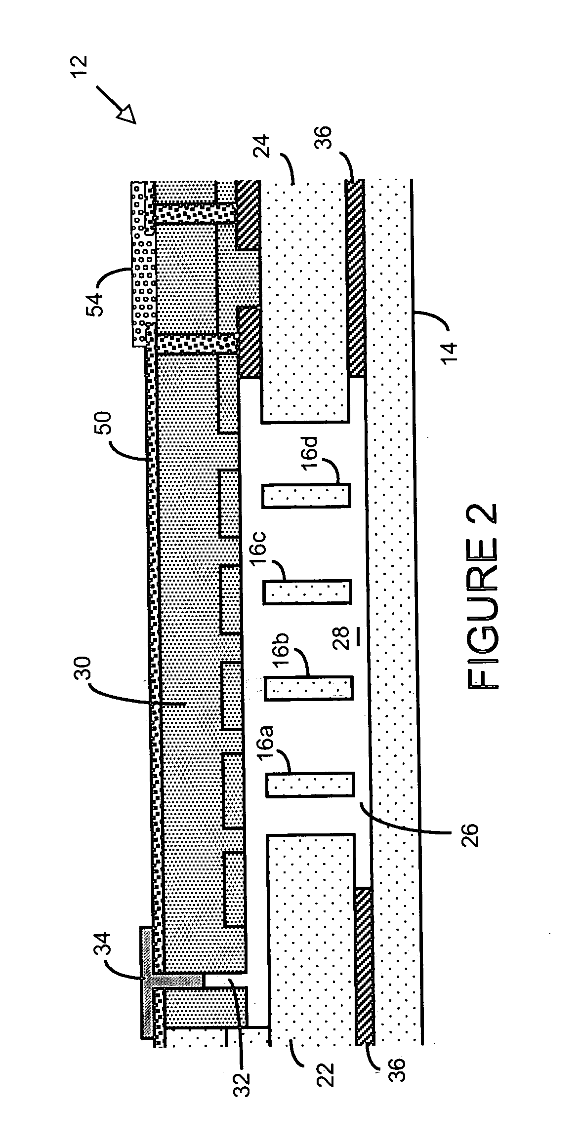
[0053] There are many inventions described and illustrated herein. In one aspect, the present invention is directed to a thin film or wafer encapsulated MEMS, and technique of fabricating or manufacturing a thin film or wafer encapsulated MEMS employing the anti-stiction techniques of the present invention. In one embodiment, after encapsulation of the MEMS, an anti-stiction channel is formed in the encapsulation layer(s) and / or the substrate thereby providing “access” to the chamber containing some or all of the active members or electrodes of the mechanical structures of the MEMS. Thereafter, an anti-stiction fluid (for example, gas or gas-vapor) is introduced into the chamber via the anti-stiction channel. The anti-stiction fluid may deposit on one, some or all of the active members or electrodes of the mechanical structures thereby providing an anti-stiction layer (for example, a monolayer coating or self-assembled monolayer) and / or out-gassing molecules on such members or elect...


PUM

PropertyMeasurementUnit
Pressureaaaaaaaaaa
Mechanical propertiesaaaaaaaaaa

Abstract

There are many inventions described and illustrated herein. In one aspect, present invention is directed to a thin film or wafer encapsulated MEMS, and technique of fabricating or manufacturing a thin film or wafer encapsulated MEMS employing the anti-stiction techniques of the present invention. In one embodiment, after encapsulation of the MEMS, an anti-stiction channel is formed thereby providing “access” to the chamber containing some or all of the active members or electrodes of the mechanical structures of the MEMS. Thereafter, an anti-stiction fluid (for example, gas or gas-vapor) is introduced into the chamber via the anti-stiction channel. The anti-stiction fluid may deposit on one, some or all of the active members or electrodes of the mechanical structures thereby providing an anti-stiction layer (for example, a monolayer coating or self-assembled monolayer) and / or out-gassing molecules on such members or electrodes. After introduction and / or application of the anti-stiction fluid, the anti-stiction channel may be sealed, capped, plugged and / or closed to define and control the mechanical damping environment within the chamber. In this regard, sealing, capping and / or closing the chamber establishes the environment within the chamber containing and / or housing the mechanical structures. This environment provides the predetermined, desired and / or selected mechanical damping of the mechanical structure as well as suitable hermeticity. The parameters (for example, pressure) of the final encapsulated fluid (for example, a gas or a gas vapor) in which the mechanical structures are to operate may be controlled, selected and / or designed to provide a desired and / or predetermined operating environment.

Description

[0001] This invention relates to electromechanical systems and techniques for fabricating microelectromechanical and / or nanoelectromechanical systems; and more particularly, in one aspect, to fabricating or manufacturing microelectromechanical and nanoelectromechanical systems having mechanical structures that are encapsulated using thin film or wafer bonding encapsulation techniques, and including suitable anti-stiction characteristics. [0002] Microelectromechanical systems (“MEMS”), for example, gyroscopes, resonators and accelerometers, utilize micromachining techniques (i.e., lithographic and other precision fabrication techniques) to reduce mechanical components to a scale that is generally comparable to microelectronics. MEMS typically include a mechanical structure fabricated from or on, for example, a silicon substrate using micromachining techniques. [0003] MEMS often operate through the movement of certain elements or electrodes, relative to fixed or stationary electrodes,...

Claims


Application Information

Patent Timeline
05 May 2005
Publication
US20050095833A1
IPC
B62K1/00; B81C1/00; H01L; H01L21/00; H01L21/44; H01L29/82
CPC
B81B3/0005; B82Y30/00; B82Y10/00; B81C1/0096; H01L21/00
Inventors
LUTZ, MARKUS; PARTRIDGE, AARON