Anti-stiction technique for thin film and wafer-bonded encapsulated microelectromechanical systems

a microelectromechanical and anti-stiction technology, applied in the direction of instruments, acceleration measurement using interia forces, cycles, etc., can solve the problems of stiction typically rendering the mems inoperative, the gap distance between the moving electrode and the stationary or fixed electrode changes, and the electrodes may become stuck

Inactive Publication Date: 2005-08-16
ROBERT BOSCH GMBH
View PDF31 Cites 96 Cited by
  • Summary
  • Abstract
  • Description
  • Claims
  • Application Information

AI Technical Summary

Benefits of technology

[0006]In the context of the semiconductor or glass-like substrate packaging technique, the substrate of the mechanical structure may be bonded to another substrate whereby the bonded substrates form a chamber within which the mechanical structure resides. In this way, the operating environment of the mechanical structure may be controlled and the structure itself protected from, for example, inadvertent contact. The two bonded substrates may or may not be the primary package for the MEMS as well.

Problems solved by technology

This movement tends to result in a change in gap distances between moving electrodes and stationary or fixed electrodes (for example, the gap between opposing electrodes).
Under certain conditions, for example, during operation, the deflectable or moveable electrode may contact the stationary or fixed electrode and the electrodes may become stuck.
This may be the result of, for example, rapid, sudden and / or violent movement of the MEMS.
Stiction typically renders the MEMS inoperative.
In wafer level packaging of mechanical structures, however, the thin encapsulation film is often deposited at high temperatures.
Conventional lubricants or passivation layers are susceptible to destruction when subjected to those temperatures required for fabricating the thin film encapsulation or integrated circuits.
Thus, after encapsulation, the mechanical structures are more prone to stiction as a consequence of the post-mechanical structure processing.

Method used


Image

  • Anti-stiction technique for thin film and wafer-bonded encapsulated microelectromechanical systems
  • Anti-stiction technique for thin film and wafer-bonded encapsulated microelectromechanical systems
  • Anti-stiction technique for thin film and wafer-bonded encapsulated microelectromechanical systems

Examples


Embodiment Construction

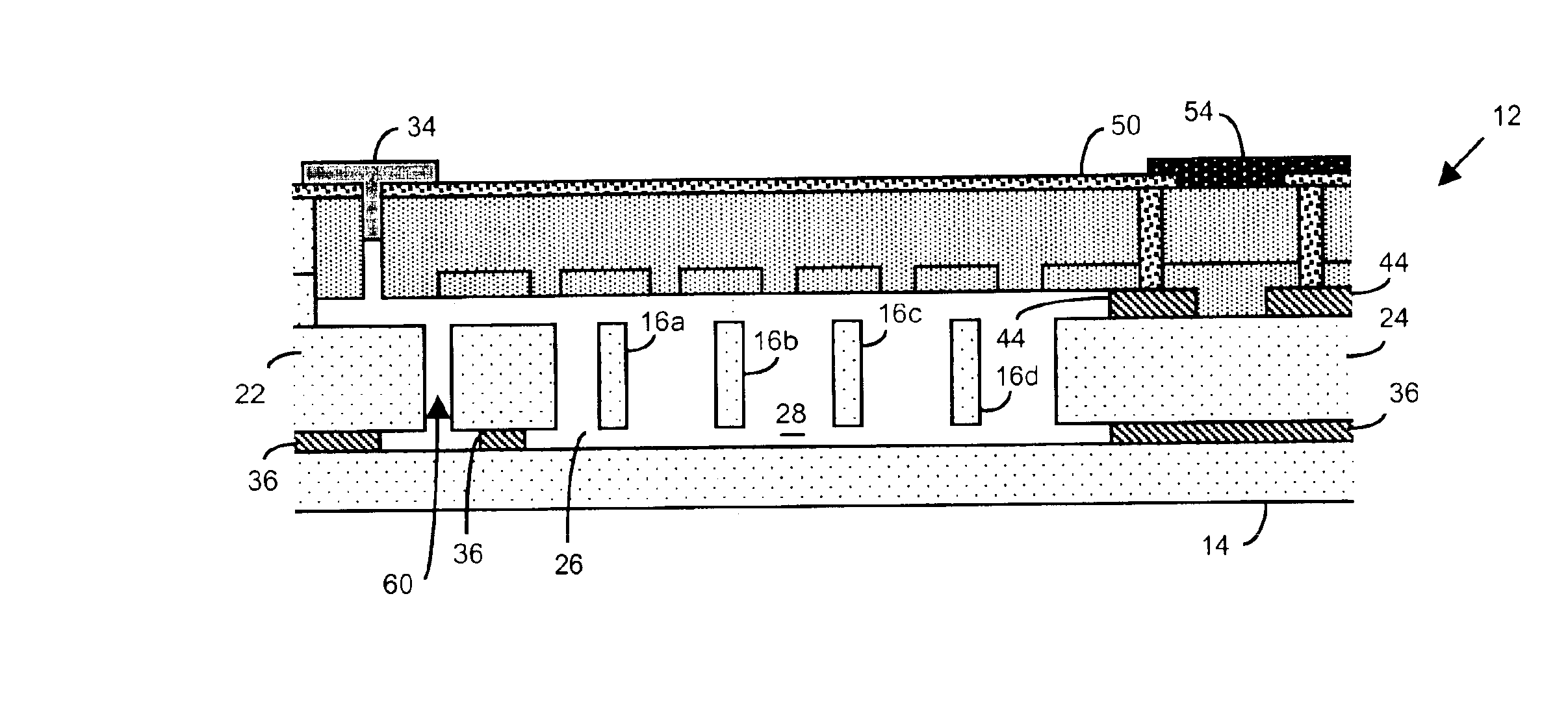
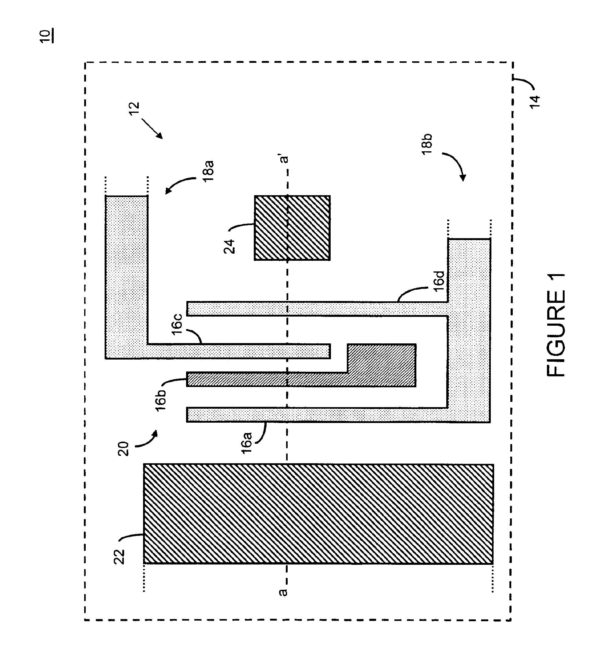
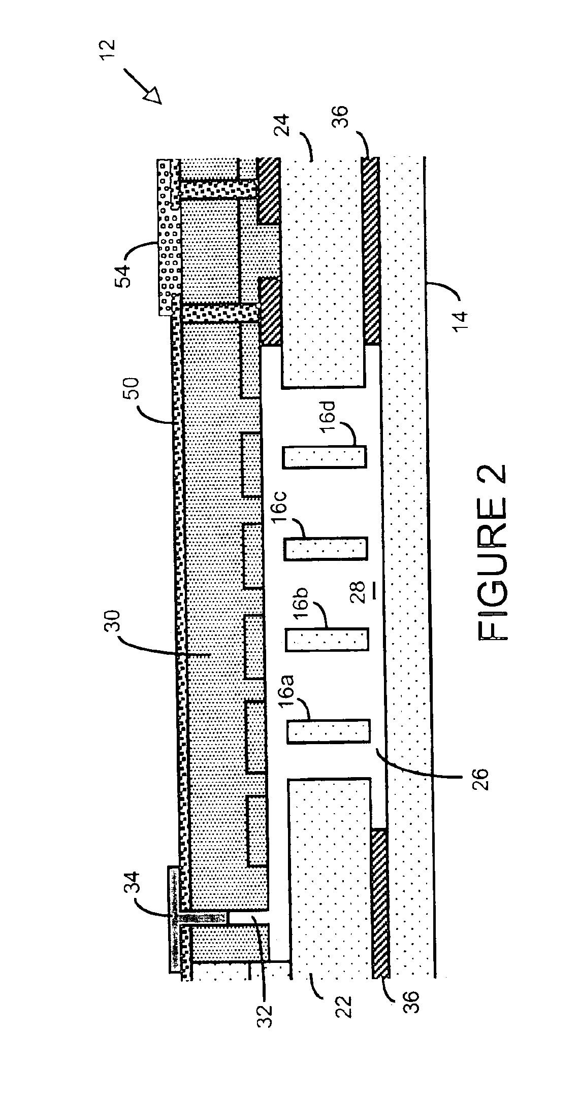
[0053]There are many inventions described and illustrated herein. In one aspect, the present invention is directed to a thin film or wafer encapsulated MEMS, and technique of fabricating or manufacturing a thin film or wafer encapsulated MEMS employing the anti-stiction techniques of the present invention. In one embodiment, after encapsulation of the MEMS, an anti-stiction channel is formed in the encapsulation layer(s) and / or the substrate thereby providing “access” to the chamber containing some or all of the active members or electrodes of the mechanical structures of the MEMS. Thereafter, an anti-stiction fluid (for example, gas or gas-vapor) is introduced into the chamber via the anti-stiction channel. The anti-stiction fluid may deposit on one, some or all of the active members or electrodes of the mechanical structures thereby providing an anti-stiction layer (for example, a monolayer coating or self-assembled monolayer) and / or out-gassing molecules on such members or electr...


PUM

PropertyMeasurementUnit
diameteraaaaaaaaaa
diameteraaaaaaaaaa
diameteraaaaaaaaaa

Abstract

There are many inventions described and illustrated herein. In one aspect, there is described a thin film or wafer encapsulated MEMS, and technique of fabricating or manufacturing a thin film or wafer encapsulated MEMS employing anti-stiction techniques. In one embodiment, after encapsulation of the MEMS, an anti-stiction channel is formed thereby providing “access” to the chamber containing some or all of the active members or electrodes of the mechanical structures. Thereafter, an anti-stiction fluid (for example, gas or gas-vapor) is introduced into the chamber via the anti-stiction channel. The anti-stiction fluid may deposit on one, some or all of the active members of the mechanical structures thereby providing an anti-stiction layer (for example, a monolayer coating or self-assembled monolayer) and / or out-gassing molecules on such members or electrodes. After introduction and / or application of the anti-stiction fluid, the anti-stiction channel may be sealed, capped, plugged and / or closed.

Description

[0001]This invention relates to electromechanical systems and techniques for fabricating microelectromechanical and / or nanoelectromechanical systems; and more particularly, in one aspect, to fabricating or manufacturing microelectromechanical and nanoelectromechanical systems having mechanical structures that are encapsulated using thin film or wafer bonding encapsulation techniques, and including suitable anti-stiction characteristics.[0002]Microelectromechanical systems (“MEMS”), for example, gyroscopes, resonators and accelerometers, utilize micromachining techniques (i.e., lithographic and other precision fabrication techniques) to reduce mechanical components to a scale that is generally comparable to microelectronics. MEMS typically include a mechanical structure fabricated from or on, for example, a silicon substrate using micromachining techniques.[0003]MEMS often operate through the movement of certain elements or electrodes, relative to fixed or stationary electrodes, of t...

Claims


Application Information

Patent Timeline
Patent Type & Authority Patents(United States)
IPC IPC(8): B62K1/00H01L21/02H01L21/00H01L21/44H01L29/82H01L29/66B81C1/00H01L
CPCB81B3/0005B81C1/0096B82Y10/00B82Y30/00H01L21/00
Inventor LUTZ, MARKUSPARTRIDGE, AARON
Owner ROBERT BOSCH GMBH
Why Eureka
Try Eureka