

Semiconductor device and its manufacture method capable of preventing short circuit of electrodes when semiconductor device is mounted on sub-mount substrate
a semiconductor device and manufacturing method technology, applied in the manufacture of printed circuits, non-metallic protective coating applications, printed element electric connection formation, etc., can solve the problem of inability to prevent short circuits, and achieve the effect of preventing short circuits between electrodes
- Summary
- Abstract
- Description
- Claims
- Application Information
AI Technical Summary
Benefits of technology
Problems solved by technology
Method used
Image

Examples
first embodiment
[0030] With reference to FIGS. 1 and 2, description will be made on a semiconductor device and its manufacture method according to the
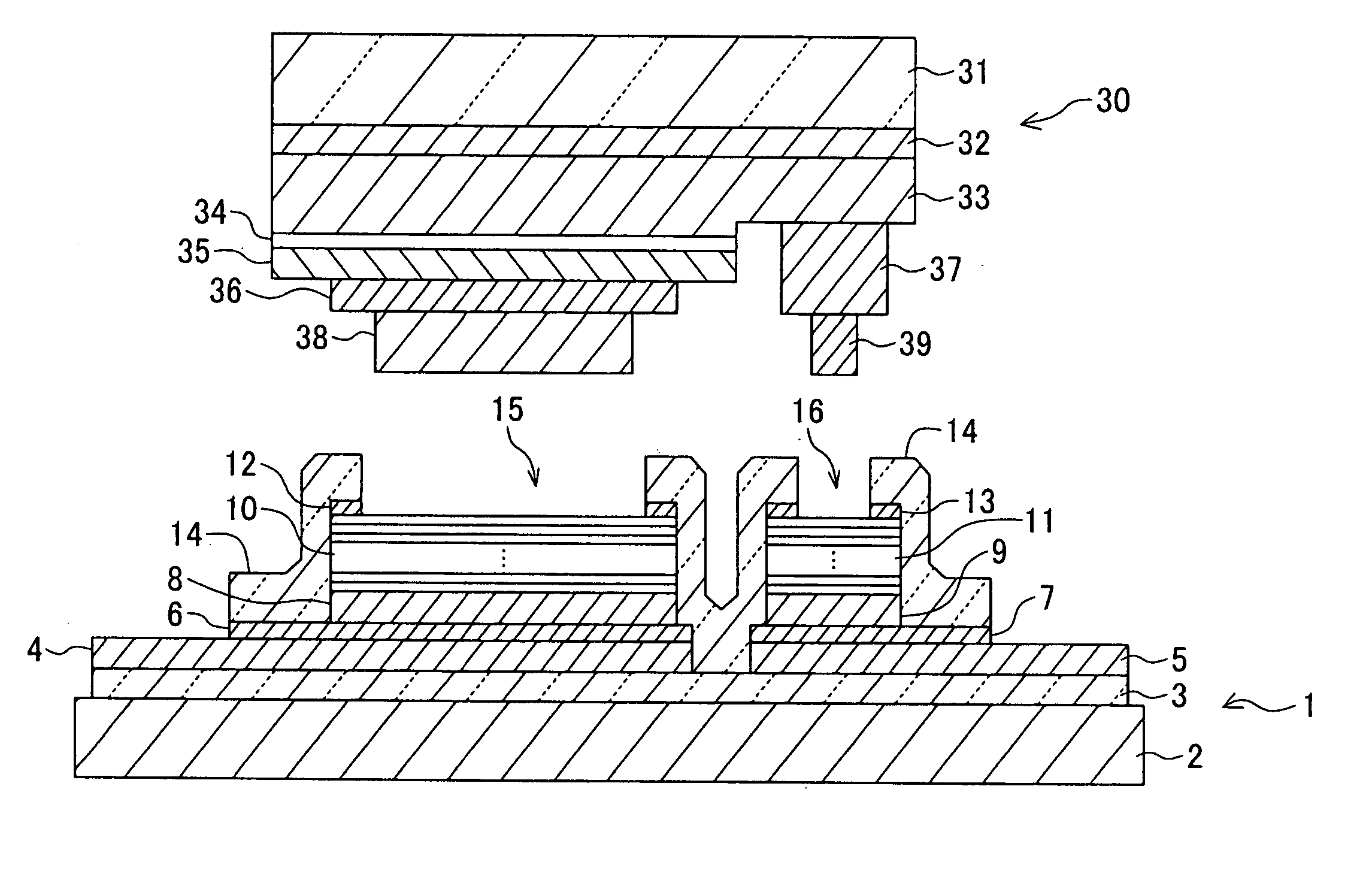
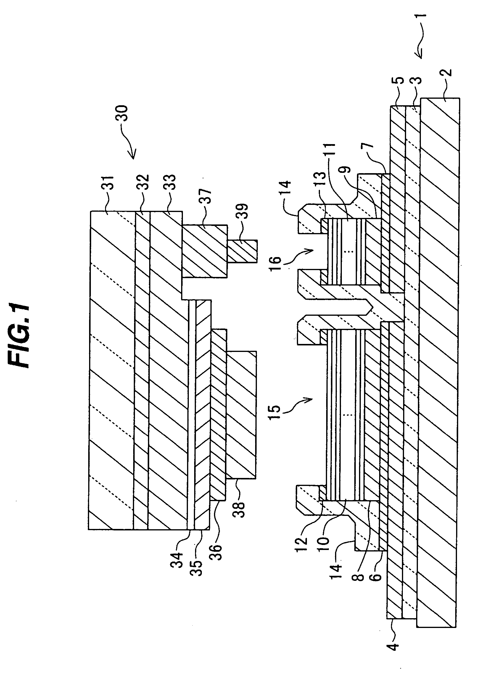
[0031] As shown in FIG. 1, the semiconductor device of the first embodiment is constituted of a sub-mount substrate 1 and a semiconductor light emitting device 30.
[0032] The structure of the sub-mount substrate 1 will be described. On the principal surface of an underlying substrate 2 made of silicon or the like, an insulating film 3 is formed which is made of silicon oxide and has a thickness of 300 nm. Formed on the insulating film 3 are an extension layer 4 to be connected to a p-side electrode of the semiconductor light emitting device 30 and an extension layer 5 to be connected to an n-side electrode. The extension layers 4 and 5 have a two-layer structure of, for example, a titanium (Ti) layer having a thickness of 10 nm and a gold (Au) layer having a thickness of 1000 nm. The two-layer structure of the extension layers 4 and 5 may be made of a...
third embodiment
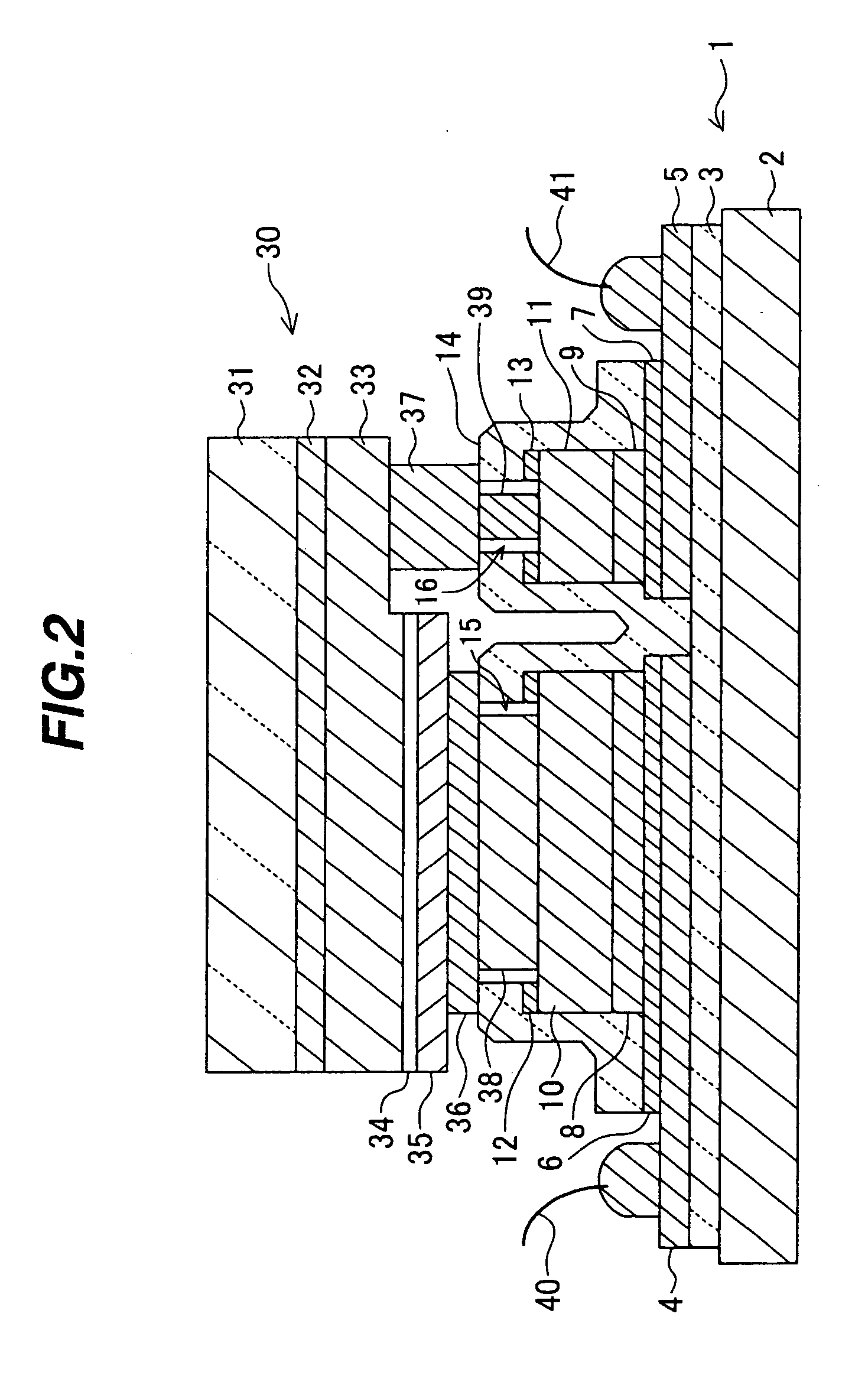
[0083] With reference to FIG. 5, a semiconductor device will be described. FIG. 5 is a cross sectional view showing the state before a semiconductor light emitting device 30a is mounted on a sub-mount substrate 1a.
[0084] Description will be made on the structure of the sub-mount substrate 1a and its manufacture method. Similar to the first embodiment, an insulating film 3, extension layers 4 and 5 and adhesion layers 6 and 7 are formed on the principal surface of a silicon substrate 2.
[0085] A p-side pad electrode (connection member on the sub-mount substrate side) 61 is formed on a partial surface of the adhesion layer 6, and an adhesion layer 63 is formed on the p-side pad electrode 61. An n-side pad electrode 62 is formed on a partial surface of the adhesion layer 5, and an adhesion layer 64 is formed on the n-side pad electrode 62. The pad electrodes 61 and 62 have a four-layer structure of a Ti layer having a thickness of 10 nm, an Au layer having a thickness of 100 nm, a Pt...
second embodiment
[0094] As shown in FIG. 6, similar to the second embodiment shown in FIG. 3, the surface of the semiconductor light emitting device 30a facing the sub-mount substrate 1a may be covered with a protective film 75 of silicon oxide. An adhesion layer 76 is disposed between the protective film 75 and the upper surface of the barrier layer 71, and an adhesion layer 77 is disposed between the protective film 75 and the upper surface of the barrier layer 72. In the state that the semiconductor light emitting device 30a is mounted on the sub-mount substrate 1a, the upper surface of the protective film 75 contacts the upper surface of the levee film 14a in the peripheral areas of the openings 15a and 16a. The connection members 73 and 74 are made thicker by the total thickness of the adhesion layer 76 and protective film 75 than the thickness of the connections members 73 and 74 shown in FIG. 5.
[0095] With reference to FIG. 7, a semiconductor device of the fourth embodiment will be described....
PUM
 Abstract
Description
Claims
Application Information