Tamper evident package
a packaging and packaging technology, applied in the field of packaging, can solve the problems of high percentage of tampered semiconductor devices and related products sold to end users, distributors or other buyers in retail packaging, and achieve the effect of reducing the number of tampered products
- Summary
- Abstract
- Description
- Claims
- Application Information
AI Technical Summary
Problems solved by technology
Method used
Image
Examples
Embodiment Construction
[0009] In the following detailed description, reference is made to the accompanying drawings which form a part hereof wherein like numerals designate like parts throughout, and in which is shown by way of illustration specific embodiments in which the invention may be practiced. It is to be understood that other embodiments may be utilized and structural or logical changes may be made without departing from the scope of the present invention. Therefore, the following detailed description is not to be taken in a limiting sense, and the scope of the present invention is defined by the appended claims and their equivalents.
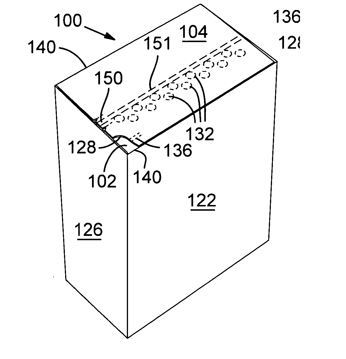
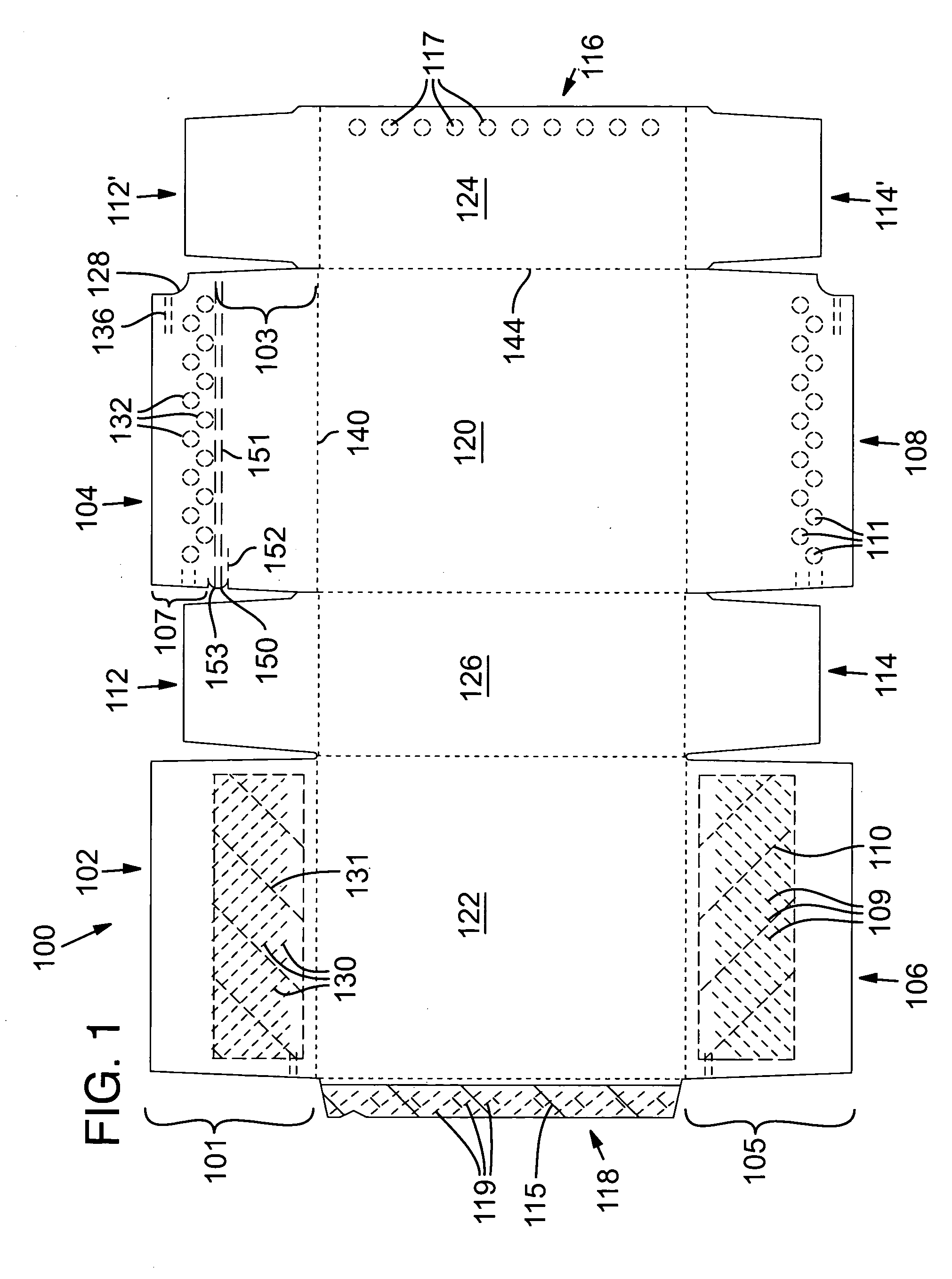
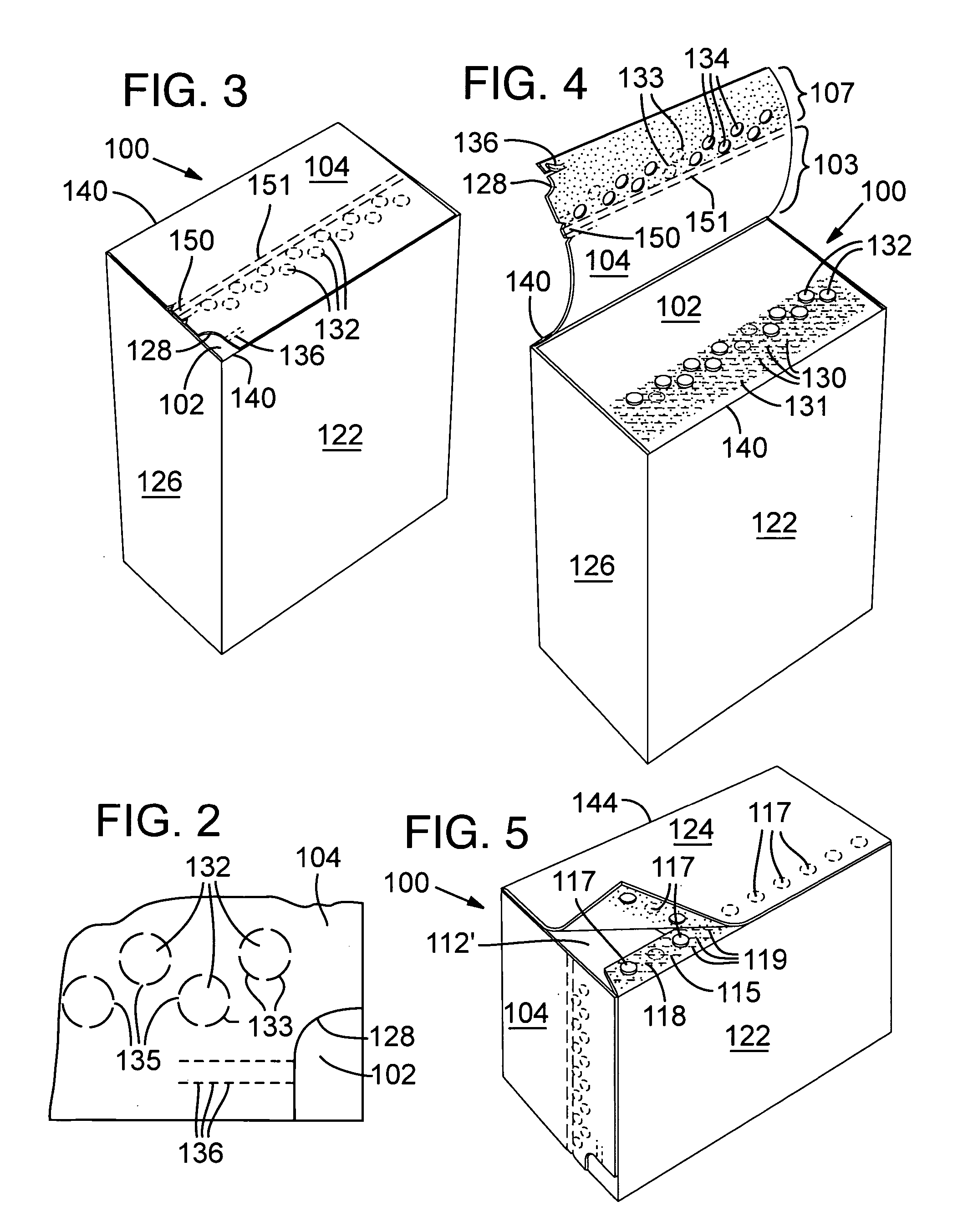
[0010]FIG. 1 illustrates a plan view of a tamper evident package in accordance with an embodiment of the present invention. A package 100 as shown is in its pre-formed configuration such that it lies substantially flat. Package 100 has several features which when used in combination with an adhesive, may resist the ability of the package 100 to be opened without at ...
PUM
 Abstract
Description
Claims
Application Information


