Voltage level shifting circuit and method

a voltage level shifting and voltage level technology, applied in logic circuits, logic circuit coupling/interface arrangements, pulse techniques, etc., can solve the problems of increasing the voltage difference between input and output signals, affecting the performance of the voltage level shifting circuit b>100/b>, etc., and achieve the effect of higher output voltage level

Inactive Publication Date: 2005-12-15
MICRON TECH INC +1
View PDF18 Cites 5 Cited by
  • Summary
  • Abstract
  • Description
  • Claims
  • Application Information

AI Technical Summary

Benefits of technology

[0006] The present invention is directed to a voltage level shifting circuit and method for shifting the voltage level of an input signal and provide an output signal having a higher output voltage level. In one aspect of the invention, the voltage level shifting circuit includes a first current path from a voltage supply to ground having a first input signal node to which an input signal is coupled, a first output signal node from which an output signal is provided, a first pull-up node, and a first switching node. The first discharge path couples the voltage supply to the first output signal node under control of the first pull-up node and couples the switching node to ground in response to the input signal. The voltage level shifting circuit further includes a second current path from the voltage supply to ground having a second input signal node to which a complementary input signal is coupled, a second output signal node from which a complementary output signal provided, a second pull-up node coupled to the first switching node, and a second switching node coupled to the first pull-up node. The second discharge path couples the voltage supply to the second output signal node under control of the second pull-up node and couples the second switching node to ground in response to the complementary input signal. A third current path is included in the voltage level shifting circuit to couple the output signal node to ground in response to the input signal.

Problems solved by technology

The performance of the conventional voltage level shifting circuit 100 begins to suffer as the voltage difference between the input and output signals becomes greater.

Method used


Image

  • Voltage level shifting circuit and method
  • Voltage level shifting circuit and method
  • Voltage level shifting circuit and method

Examples


Embodiment Construction

[0013] Embodiments of the present invention are directed to voltage level shifting circuits and methods that can be used for shifting the voltage level of an input signal to provide an output signal having a higher output voltage level where the difference between the voltage levels of the input and output signals is large. Certain details are set forth below to provide a sufficient understanding of the invention. However, it will be clear to one skilled in the art that the invention may be practiced without these particular details. In other instances, well-known circuits, control signals, and timing protocols have not been shown in detail in order to avoid unnecessarily obscuring the invention.

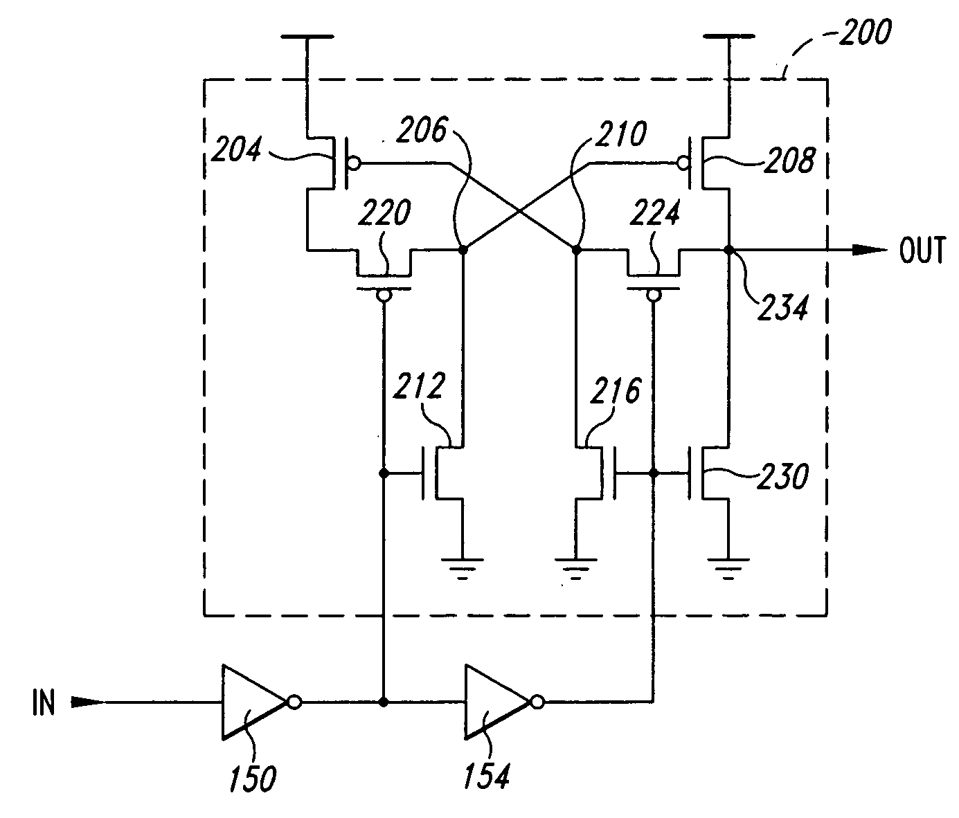
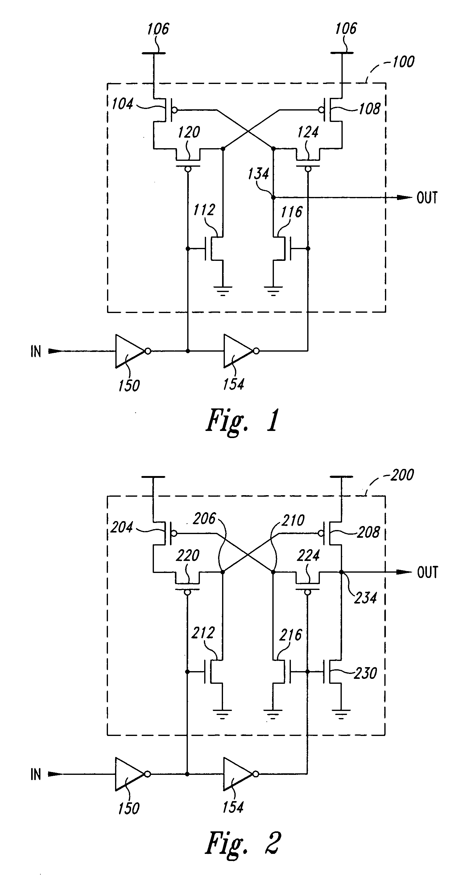
[0014]FIG. 2 illustrates a voltage level shifting circuit 200 according to an embodiment of the present invention. The voltage level shifting circuit 200 translates an input signal IN having an input voltage level V1 to an output signal OUT having an output voltage level V2. The voltage lev...


PUM


Abstract

A voltage level shifting circuit and method that can be used for shifting the voltage level of an input signal to provide an output signal having a higher output voltage level. The voltage level shifting circuit includes pull-up transistors that are switched OFF by the voltage of a pair of switching nodes and not the voltage at the output node. The speed at which the pull-up transistors can be switched OFF is decoupled to some extent from the speed at which the voltage at the output node changes. Additionally, having the output node separated from the nodes that switch the pull-up transistors OFF further allows for dimensions of the various transistors of the voltage level shifting circuit to be scaled advantageously.

Description

TECHNICAL FIELD [0001] The present invention relates to voltage level shifting circuits, and more particularly, to a voltage level shifting circuit and method that can be used for shifting the voltage level of an input signal to provide an output signal having a higher output voltage level where the difference between the voltage levels of the input and output signals is large. BACKGROUND OF THE INVENTION [0002]FIG. 1 illustrates a conventional voltage level shifting circuit 100 for translating an input signal IN having an input voltage level V1 to an output signal OUT having an output voltage level V2. The voltage level shifting circuit 100 includes p-channel MOS (PMOS) pull-up transistors 104 and 108 coupled to a voltage supply providing the voltage level V2. Coupled to the PMOS pull-up transistors 104, 108 are PMOS load transistors 120, 124 and n-channel MOS (NMOS) pull-down transistors 112, 116, all respectively. Gates of the PMOS load transistors 120, 124 and of the NMOS pull-d...

Claims


Application Information

Patent Timeline
Patent Type & Authority Applications(United States)
IPC IPC(8): H03K3/356H03K19/0175
CPCH03K3/356113H03K3/356165
Inventor KIM, TAE H.KIRSCH, HOWARD C.
Owner MICRON TECH INC
Why Eureka
Try Eureka