Method and apparatus for defect correction in a display

US20060164407A1Inactive Publication Date: 2006-07-27EASTMAN KODAK COMPAHY

Image

  • Method and apparatus for defect correction in a display
  • Method and apparatus for defect correction in a display
  • Method and apparatus for defect correction in a display

Examples


Embodiment Construction

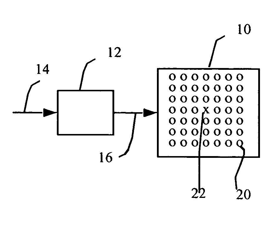
[0018] Referring to FIG. 1, one embodiment of the present invention comprises a display device having a display 10 with a plurality of pixels including one or more defective pixels 22 and one or more additional pixels 20; and a controller 12 for driving the display pixels and for transforming an input signal 14 into a compensated signal 16 for selectively modifying the output of one or more additional pixel(s) 20 in the display to compensate for the output of the defective pixel(s) 22. A defective pixel is one that does not respond as desired to a control signal. The additional pixel(s) 20 may, or may not, themselves be defective. In alternative embodiments of the present invention, the output of one additional pixel 20 may be modified or the output of several additional pixel(s) 20 may be modified, and the additional pixel(s) may be neighboring pixels to the defective pixel(s), for example surrounding the defective pixel(s) or on one side of the defective pixel(s). The display 10 o...


PUM


Abstract

A display device, comprising: a) a display having a plurality of pixels including one or more defective pixel(s) and one or more additional pixel(s); and b) a controller for driving the display pixels and for transforming an input signal into a compensated signal for selectively modifying the output of one or more additional pixel(s) in the display to compensate for the output of the defective pixel(s).

Description

FIELD OF THE INVENTION [0001] The present invention relates to displays having a plurality of light-emitting elements and, more particularly, correcting for defective light-emitting elements in the display. BACKGROUND OF THE INVENTION [0002] Flat-panel display devices, for example plasma, liquid crystal and Organic Light Emitting Diode (OLED) displays have been known for some years and are widely used in electronic devices to display information and images. Such devices employ both active-matrix and passive-matrix control schemes and can employ a plurality of light-emitting elements. The light-emitting elements are typically arranged in two-dimensional arrays with a row and a column address for each light-emitting element and having a data value associated with each light-emitting element to emit light at a brightness corresponding to the associated data value. However, such displays suffer from a variety of defects that limit the quality of the displays. In particular, displays may...

Claims


Application Information

Patent Timeline
27 Jul 2006
Publication
US20060164407A1
IPC
G09G5/00
CPC
G09G3/20; G09G2330/08; G09G2330/10
Inventors
COK, RONALD S.