

NAND ferroelectric memory cell with three-dimensional structure and preparation method thereof
a three-dimensional structure and ferroelectric memory technology, applied in the field of ferroelectric memory and integration, can solve the problem of 10sup>5 /sup>cycles fatigue property, achieve the effect of enhancing the interface property of the channel layer, reducing adverse effects, and improving the quality and uniformity of the deposited film
- Summary
- Abstract
- Description
- Claims
- Application Information
AI Technical Summary
Benefits of technology
Problems solved by technology
Method used
Image

Examples
example 1
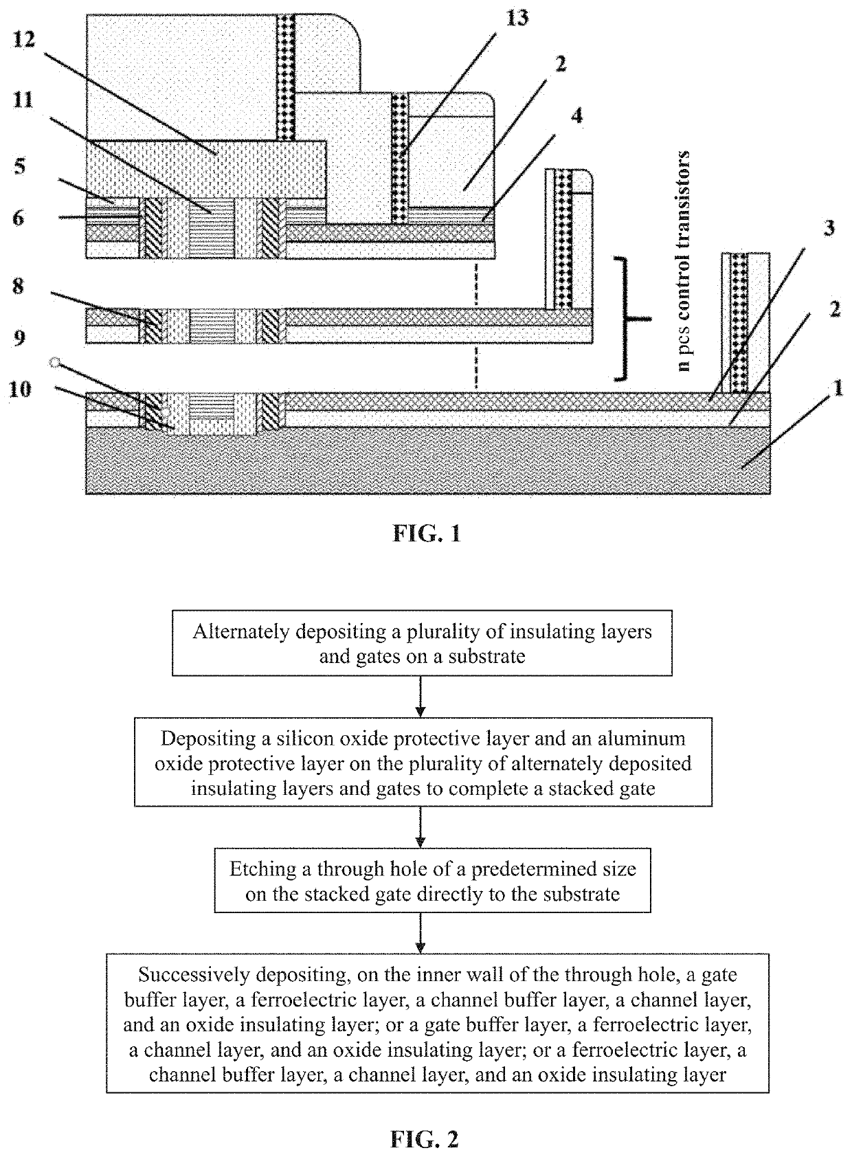
[0024]FIG. 1 is a schematic diagram of the cross-sectional structure of a NAND ferroelectric memory cell with a three-dimensional structure provided by Example 1 of the present disclosure.
[0025]As shown in FIG. 1, this example provides a NAND ferroelectric memory cell, comprising: an oxide insulating layer, a channel layer, a channel buffer layer, a ferroelectric layer, and a gate arranged successively from the inside to the outside; a channel buffer layer is arranged between the channel layer and the ferroelectric layer; and / or a gate buffer layer is arranged between the ferroelectric layer and the gate. Specifically, it comprises an oxide insulating layer, a channel layer, a channel buffer layer, a ferroelectric layer, and a gate buffer layer; or an oxide insulating layer, a channel layer, a ferroelectric layer, and a gate buffer layer; or an oxide insulating layer, a channel layer, a channel buffer layer, and a ferroelectric layer.
[0026]The memory cell of this example is configur...
example 2
[0035]FIG. 2 is a flowchart of the method for preparing a NAND ferroelectric memory cell with a three-dimensional structure provided by Example 2 of the present disclosure.
[0036]As shown in FIG. 2, this example provides a method for preparing a NAND ferroelectric memory cell, comprising: alternately depositing a plurality of insulating layers and gates on a substrate; depositing a silicon oxide protective layer and an aluminum oxide protective layer on the plurality of alternately deposited insulating layers and gates to complete a stacked gate; etching a through hole of a predetermined size on the stacked gate directly to the substrate; and successively depositing, on the inner wall of the through hole, a gate buffer layer, a ferroelectric layer, a channel buffer layer, a channel layer, and an oxide insulating layer; or a gate buffer layer, a ferroelectric layer, a channel layer, and an oxide insulating layer; or a ferroelectric layer, a channel buffer layer, a channel layer, and a...
PUM
| Property | Measurement | Unit |
|---|---|---|
| thickness | aaaaa | aaaaa |
| thickness | aaaaa | aaaaa |
| thickness | aaaaa | aaaaa |
Abstract
Description
Claims
Application Information