

Non-volatile semiconductor memory device
- Summary
- Abstract
- Description
- Claims
- Application Information
AI Technical Summary
Benefits of technology
Problems solved by technology
Method used
Image

Examples
Embodiment Construction
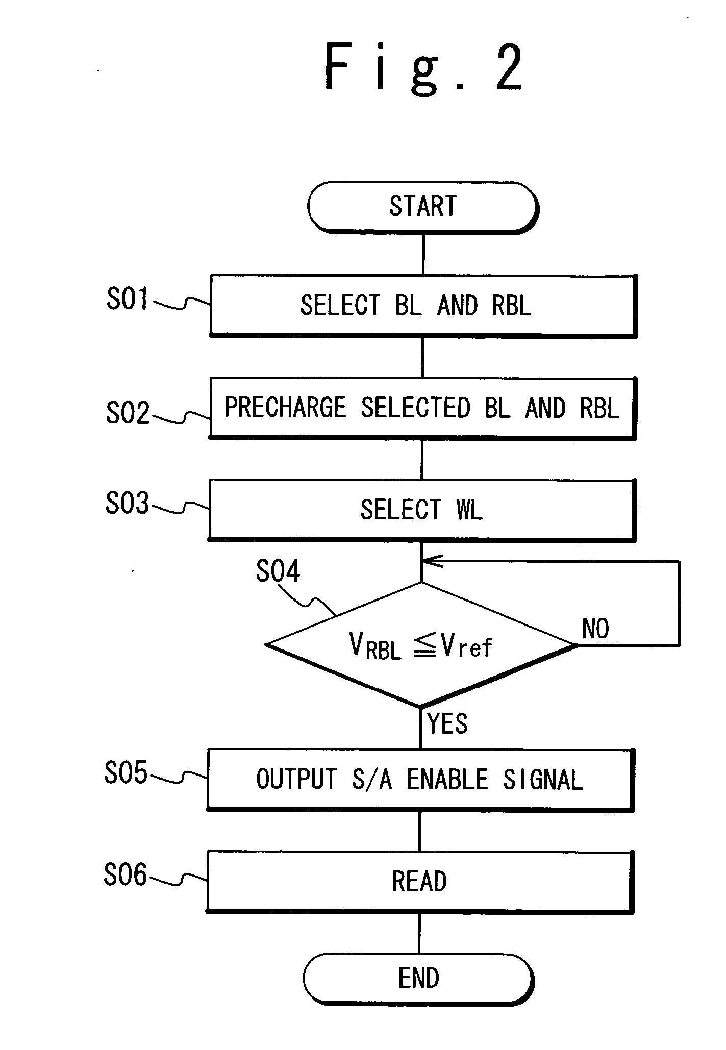
[0030] Hereinafter, a non-volatile semiconductor memory device of the present invention will be described in detail with reference to the attached drawings.
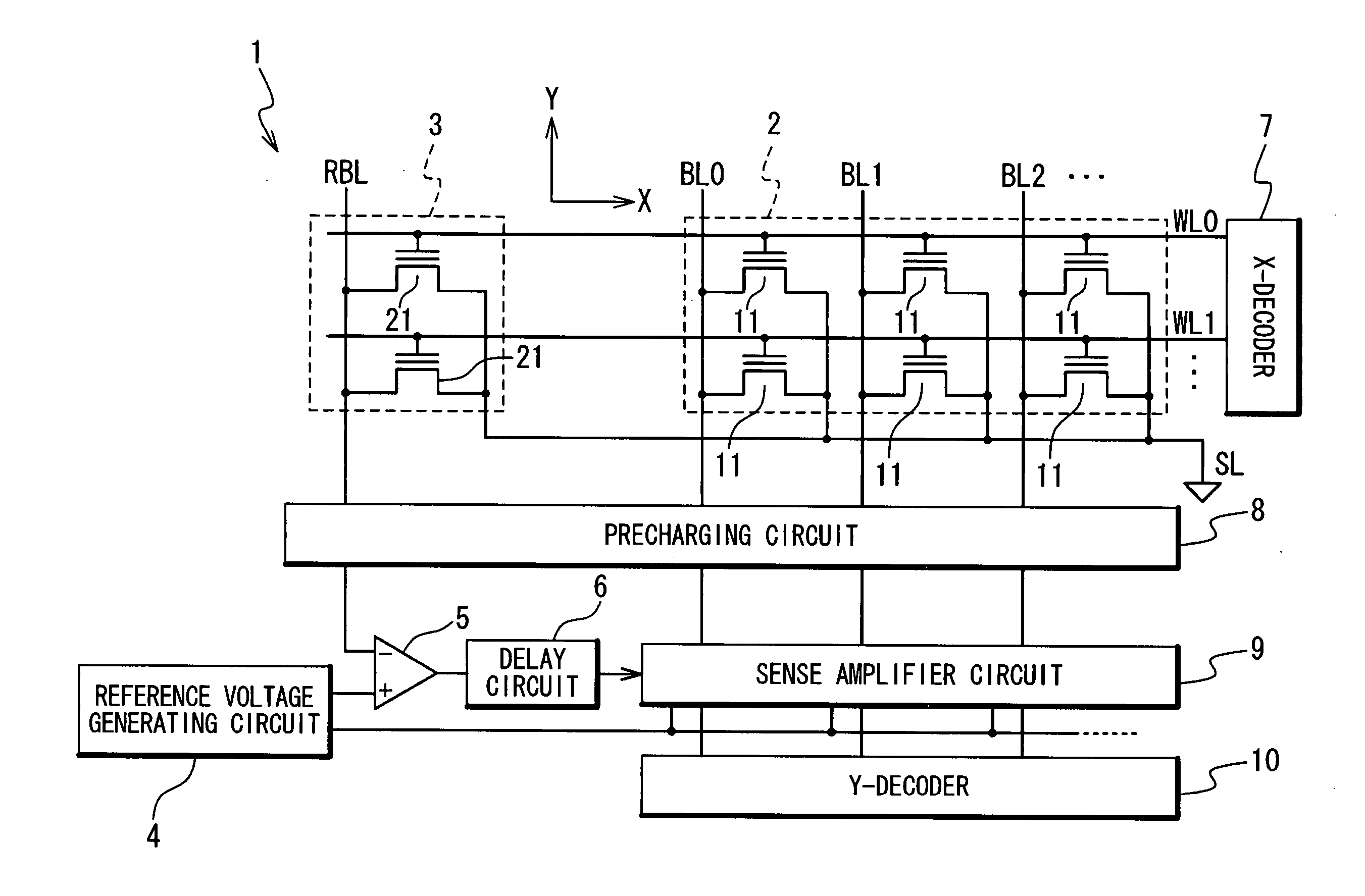
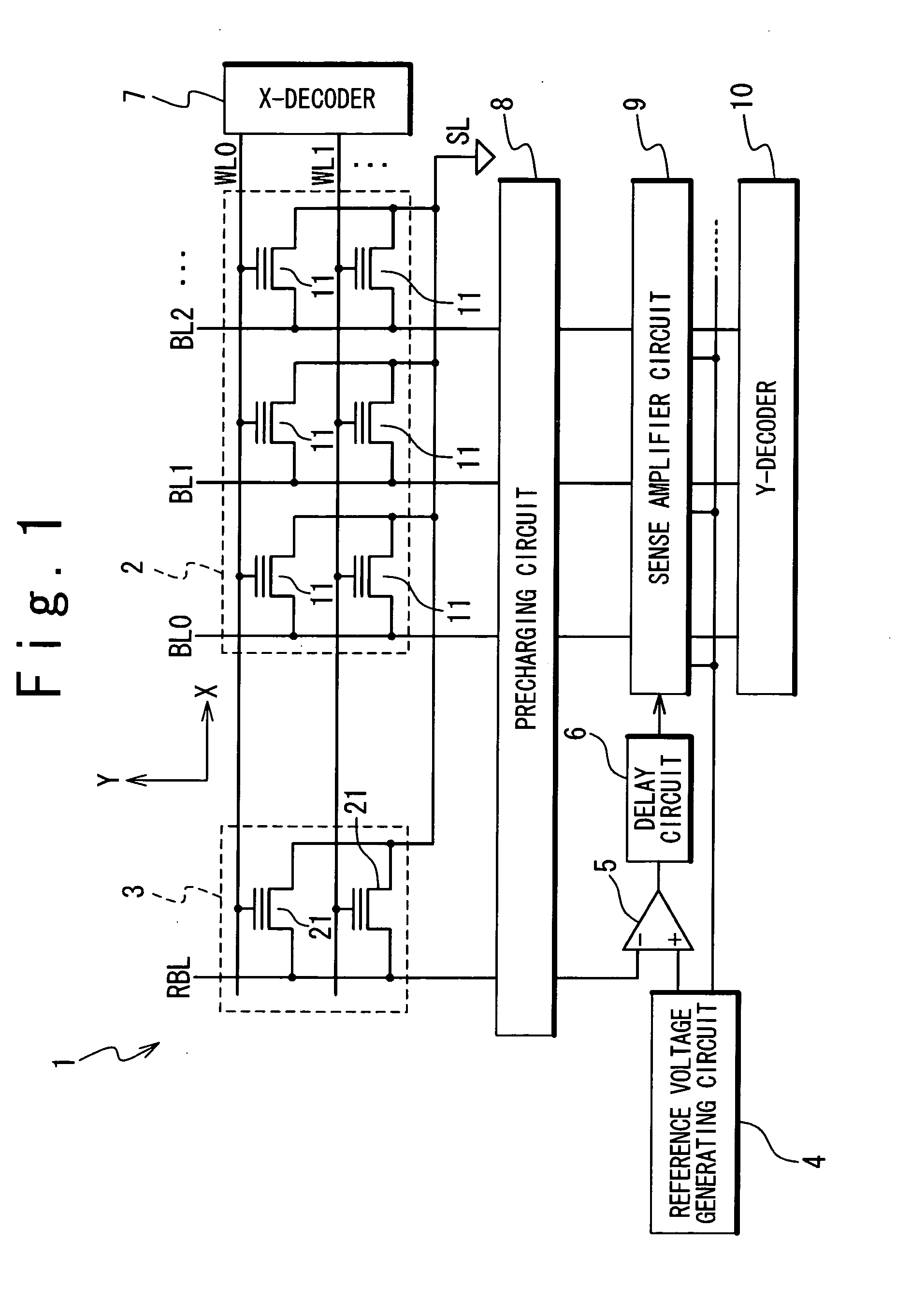
[0031] At first, the configuration of the non-volatile semiconductor memory device according to an embodiment of the present invention will be described. FIG. 1 is a block diagram showing the configuration of the non-volatile semiconductor memory device according to the embodiments of the present invention.
[0032] Referring to FIG. 1, the non-volatile semiconductor memory device 1 is provided with a memory cell array 2, a reference column 3, a reference voltage generating circuit 4, a comparator 5, a delay circuit 6, an X-decoder 7, a precharging circuit 8, a sense amplifier circuit 9 and a Y-decoder 10.
[0033] The memory cell array 2 contains a plurality of bit lines BL0, BL1, . . . , a plurality of word lines WL0, WL1, . . . , a source line SL, and a plurality of memory cells 11. The plurality of bit lines BL0, BL1, . . . exte...
PUM
 Abstract
Description
Claims
Application Information