
Spacer Patterns Using Assist Layer for High Density Semiconductor Devices
a technology of assist layer and spacer pattern, which is applied in the direction of semiconductor devices, semiconductor/solid-state device details, electrical apparatus, etc., can solve the problems of continuous pressure required to shrink the substrate area, and achieve the effect of reducing the size of the underlying dielectric layer, avoiding damage, and reducing the feature siz
- Summary
- Abstract
- Description
- Claims
- Application Information
AI Technical Summary
Benefits of technology
Problems solved by technology
Method used
Image

Examples
Embodiment Construction
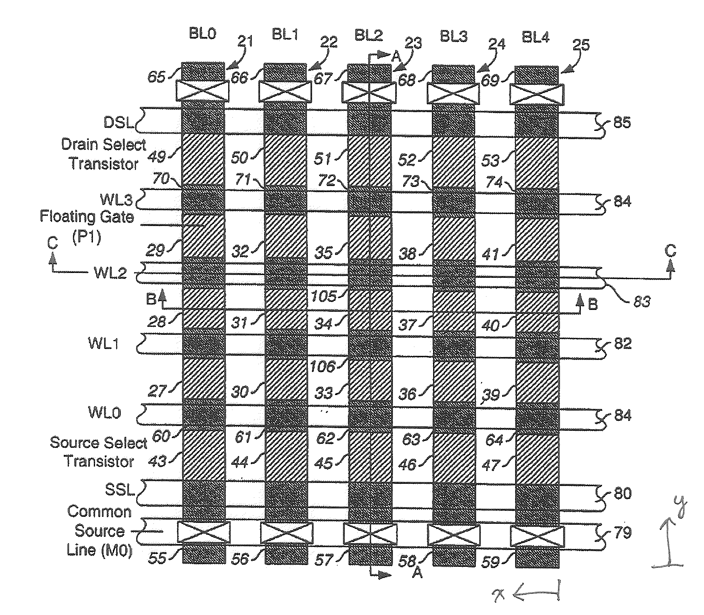
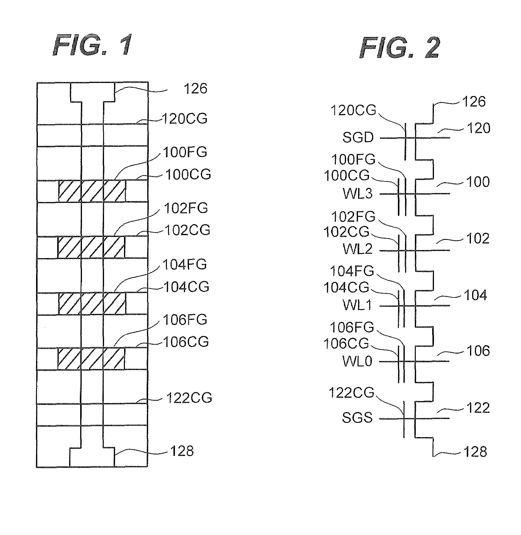
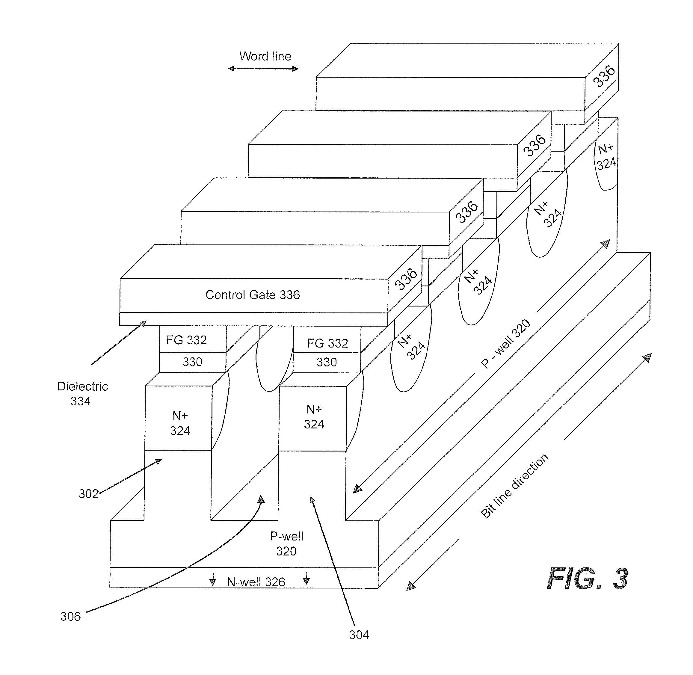
[0023]Embodiments in accordance with the present disclosure can be used in the formation of numerous types of high density semiconductor devices. A spacer and corresponding formation technique are provided to reduce the size of the fabricated elements. While not so limited, the described techniques can achieve feature sizes that are smaller than the smallest lithographically resolvable element size of the process being used. This can facilitate the high density formation of numerous types of elements in integrated semiconductor device fabrication. Various features and techniques are presented with respect to the NAND flash memory architecture. It will be appreciated from the provided disclosure that implementations of the disclosed technology are not so limited. By way of non-limiting example, embodiments in accordance with the present disclosure can provide and be used in the fabrication of a wide range of semiconductor devices, including but not limited to logic arrays, volatile m...
PUM
 Abstract
Description
Claims
Application Information