FinFET-Based Memory Testing Using Multiple Read Operations

Active Publication Date: 2018-05-10
SYNOPSYS INC
View PDF0 Cites 5 Cited by
  • Summary
  • Abstract
  • Description
  • Claims
  • Application Information

AI Technical Summary

Benefits of technology

[0010]The present invention is directed to test methodologies for detecting both known and potentially unknown FinFET-specific faults by way of implementing an efficient and reliable base set of March elements in which multiple (i.e., at least three) sequential March-type read operations are performed immediately after logic values (i.e., logic-0 or logic-1) are written into each FinFET cell of a memory array. For example, a novel test methodology might include a March-type write-1 operation followed immediately by (i.e., such that no intervening March-type elements are performed) multiple sequentially-executed March-type read-1 operations, and a March-type write-0 operation followed immediately by multiple sequentially-executed March-type read-0 operations. Alternatively, the order of the write/read operations may be reversed (i.e., the write-0-multiple-read-0 sequence may be performed before the write-1-multiple-read-1 sequence), and additional March-type tests may be included before, between and after the two sequences. It was determined experimentally that, due to the construction and configuration of FinFET cells fabricated using known process technologies, certain dynamic FinFET memory faults generate data errors when the same lo

Problems solved by technology

It was determined experimentally that, due to the construction and configuration of FinFET cells fabricated using known process technologies, certain dynamic FinFET memory faults generate data errors when the same logic value (i.e., either logic-1 or logic-0) is read multiple times consecutively.
It was discovered that, due to the symmetrical configuration utilized in FinFET memory arrays, process flaws that cause dynamic (e.g., multiple-read-0) errors in one or more first FinFETs typically can cause mirror-image dynamic (i.e., multiple-read-1) errors in one or more second FinFET cells of the memory array.
These faults are specific to Fin

Method used


Image

  • FinFET-Based Memory Testing Using Multiple Read Operations
  • FinFET-Based Memory Testing Using Multiple Read Operations
  • FinFET-Based Memory Testing Using Multiple Read Operations

Examples


Example

DETAILED DESCRIPTION OF THE DRAWINGS

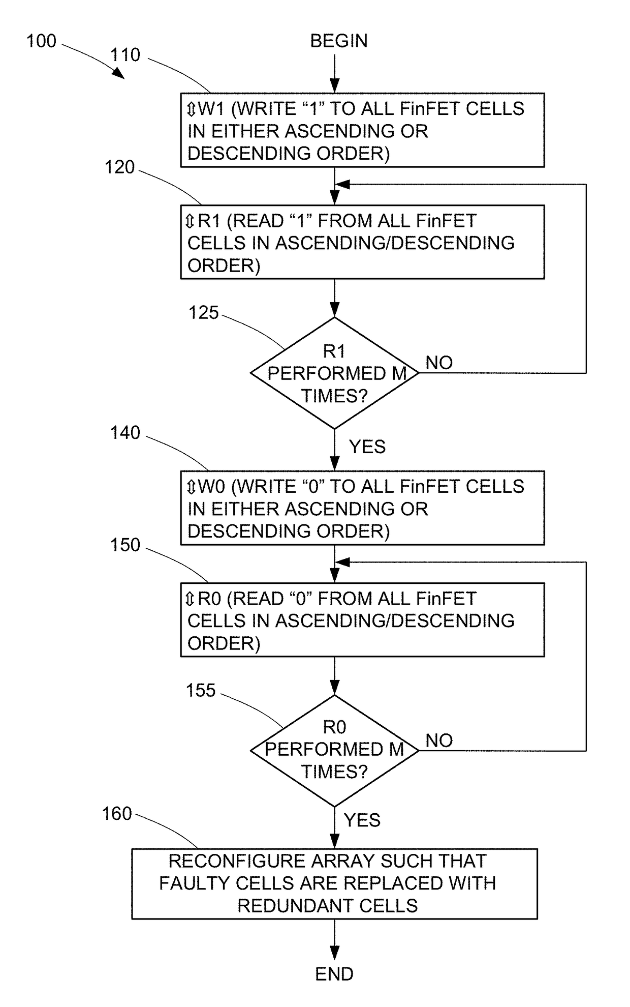
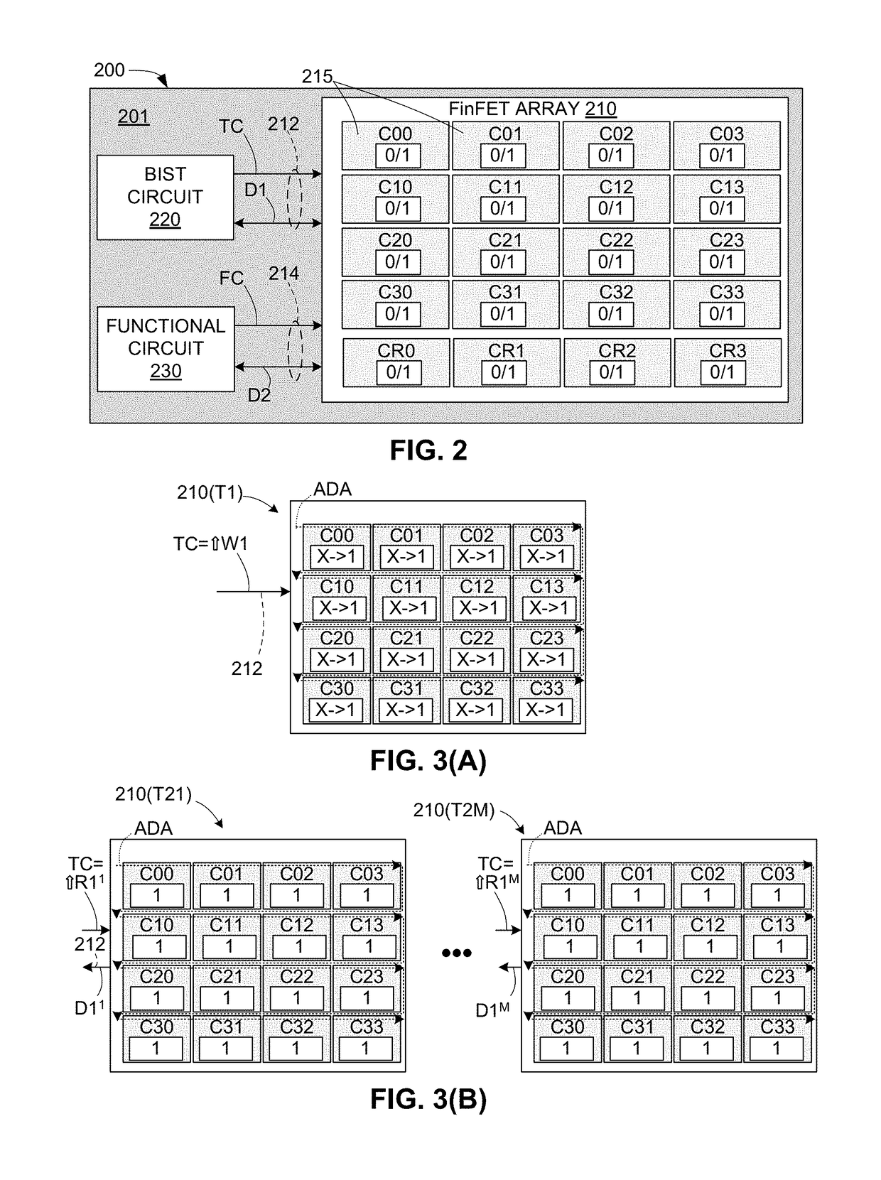
[0029]The present invention relates to an improvement in FinFET memory array testing. The following description is presented to enable one of ordinary skill in the art to make and use the invention as provided in the context of a particular application and its requirements. The terms “coupled” and “connected”, which are utilized herein, are defined as follows. The term “connected” is used to describe a direct connection between two circuit elements, for example, by way of a metal line formed in accordance with normal integrated circuit fabrication techniques. In contrast, the term “coupled” is used to describe either a direct connection or an indirect connection between two circuit elements. For example, two coupled elements may be directly connected by way of a metal line, or indirectly connected by way of an intervening circuit element (e.g., a capacitor, resistor, inductor, or by way of the source / drain terminals of a transistor). Various modif...


PUM


Abstract

A test methodologies for detecting both known and potentially unknown FinFET-specific faults by way of implementing an efficient and reliable base set of March elements in which multiple sequential March-type read operations are performed immediately after logic values (i.e., logic-0 or logic-1) are written into each FinFET cell of a memory array. For example, a March-type write-1 operation is performed, followed immediately by multiple sequentially-executed March-type read-1 operations, then a March-type write-0 operation is performed followed immediately by multiple sequentially-executed March-type read-0 operations. An optional additional March-type read-0 operation is performed before the March-type write-1 operation, and an optional additional March-type read-1 operation is performed before the March-type write-0 operation. The write-1-multiple-read-1 and write-0-multiple-read-0 sequences are performed using one or both of an increasing address order and a decreasing address order.

Description

RELATED APPLICATION[0001]This application claims priority from U.S. Provisional Patent Application 62 / 402,598, entitled “BASIC TEST PATTERNS FOR FinFET-BASED MEMORIES”, which was filed on Sep. 30, 2016, and is incorporated by reference herein.FIELD OF THE INVENTION[0002]This invention relates to testing electronic memories to identify and replace faulty memory cells in embedded memory arrays, and more particularly to modified testing algorithms optimized to identify dynamic faults in embedded FinFET-based memory arrays.BACKGROUND OF THE INVENTION[0003]Due to the ever increasing demand for cheaper, faster, more complex integrated circuit (IC) devices, IC manufacturers are replacing embedded memories based on standard planar transistor technologies with Fin Field Effect Transistor (FinFET) memories. The phrase “embedded memory” refers herein to on-chip (integrated) electronic memory devices that support a System-on-Chip (SoC) or other IC device's logic core (e.g., one or more micropro...

Claims


Application Information

Patent Timeline
IPC IPC(8): G11C29/38G11C29/36H01L27/11H01L27/092
CPCG11C29/38G11C29/36H01L27/1104H01L27/0924G11C11/41H01L27/0886H10B10/12G11C8/00H01L29/785
Inventor TSHAGHARYAN, GRIGORHARUTYUNYAN, GURGENSHOUKOURIAN, SAMVELZORIAN, YERVANT
Owner SYNOPSYS INC
Why Eureka
Try Eureka