Spacer Patterns Using Assist Layer For High Density Semiconductor Devices

a technology of assist layer and spacer pattern, which is applied in the direction of semiconductor devices, basic electric elements, electrical apparatus, etc., can solve the problems of continuous pressure required to shrink the substrate area, and achieve the effect of reducing the size of the underlying dielectric layer, avoiding damage, and reducing the feature siz

Inactive Publication Date: 2010-09-23
WODEN TECH INC
View PDF27 Cites 1 Cited by
  • Summary
  • Abstract
  • Description
  • Claims
  • Application Information

AI Technical Summary

Benefits of technology

[0013]High density semiconductor devices and methods of fabricating the same are provided in accordance with one or embodiments. Spacer fabrication techniques are utilized to form circuit elements having reduced feature sizes, which in some instances are smaller than the smallest lithographically resolvable element size of the process being used. Spacers are formed that serve as a mask for etching one or more layers to form one or more circuit elements beneath the spacers. An intervening layer having a material composition substantially similar to the spacer material is provided between a dielectric layer and an insulating sacrificial layer such as silicon nitride. When etching the sacrificial layer, the intervening layer serves as an etch stop layer to avoid damaging and reducing the size of the underlying dielectric layer. By utilizing matched material compositions, improved adhesion is provided for the spacers, thereby improving the rigidity and integrity of the spacers.

Problems solved by technology

In most integrated circuit applications, there is continual pressure to shrink the substrate area required to implement the various integrated circuit functions.

Method used


Image

  • Spacer Patterns Using Assist Layer For High Density Semiconductor Devices
  • Spacer Patterns Using Assist Layer For High Density Semiconductor Devices
  • Spacer Patterns Using Assist Layer For High Density Semiconductor Devices

Examples


Embodiment Construction

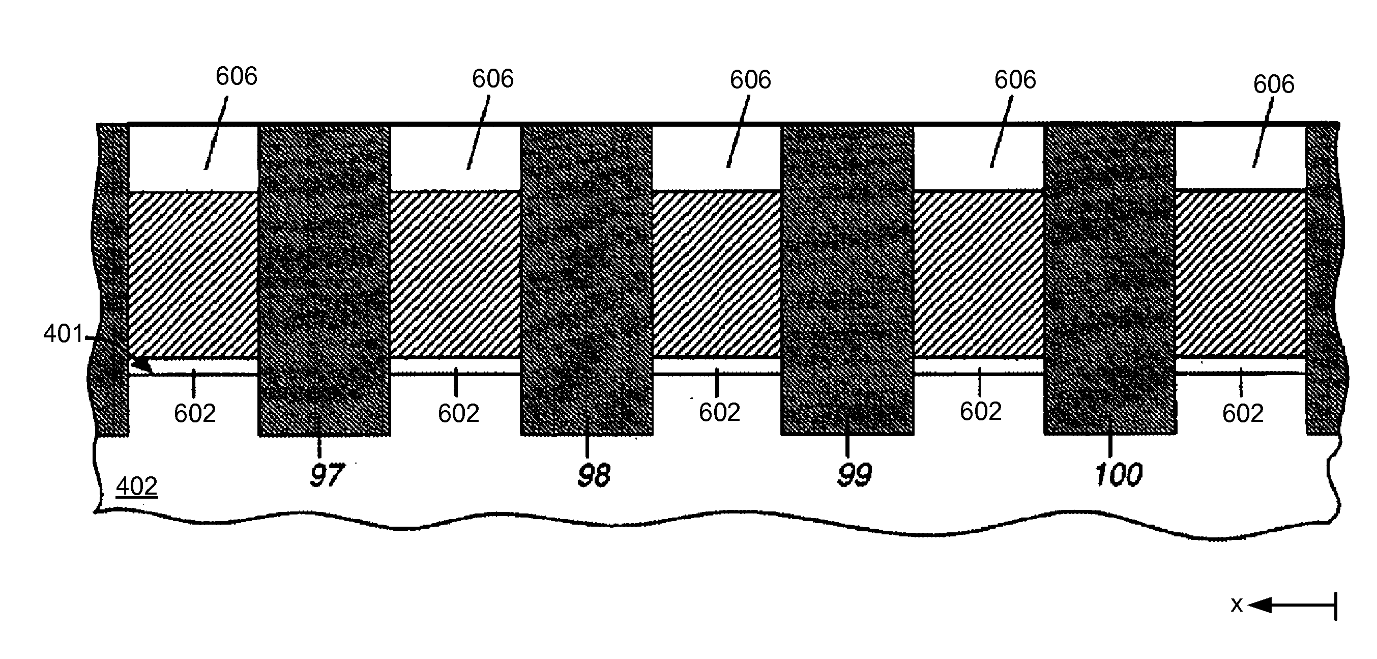
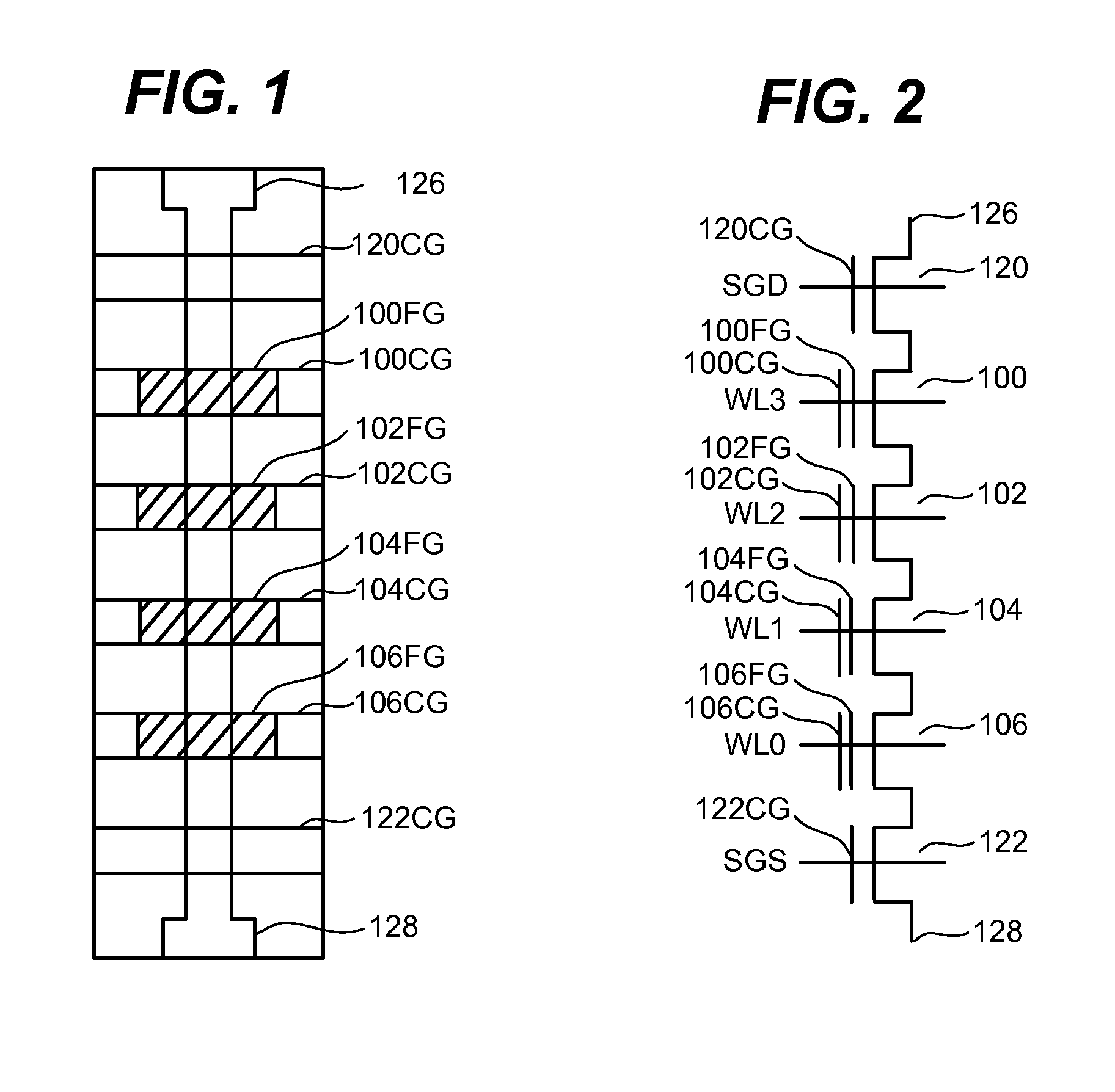
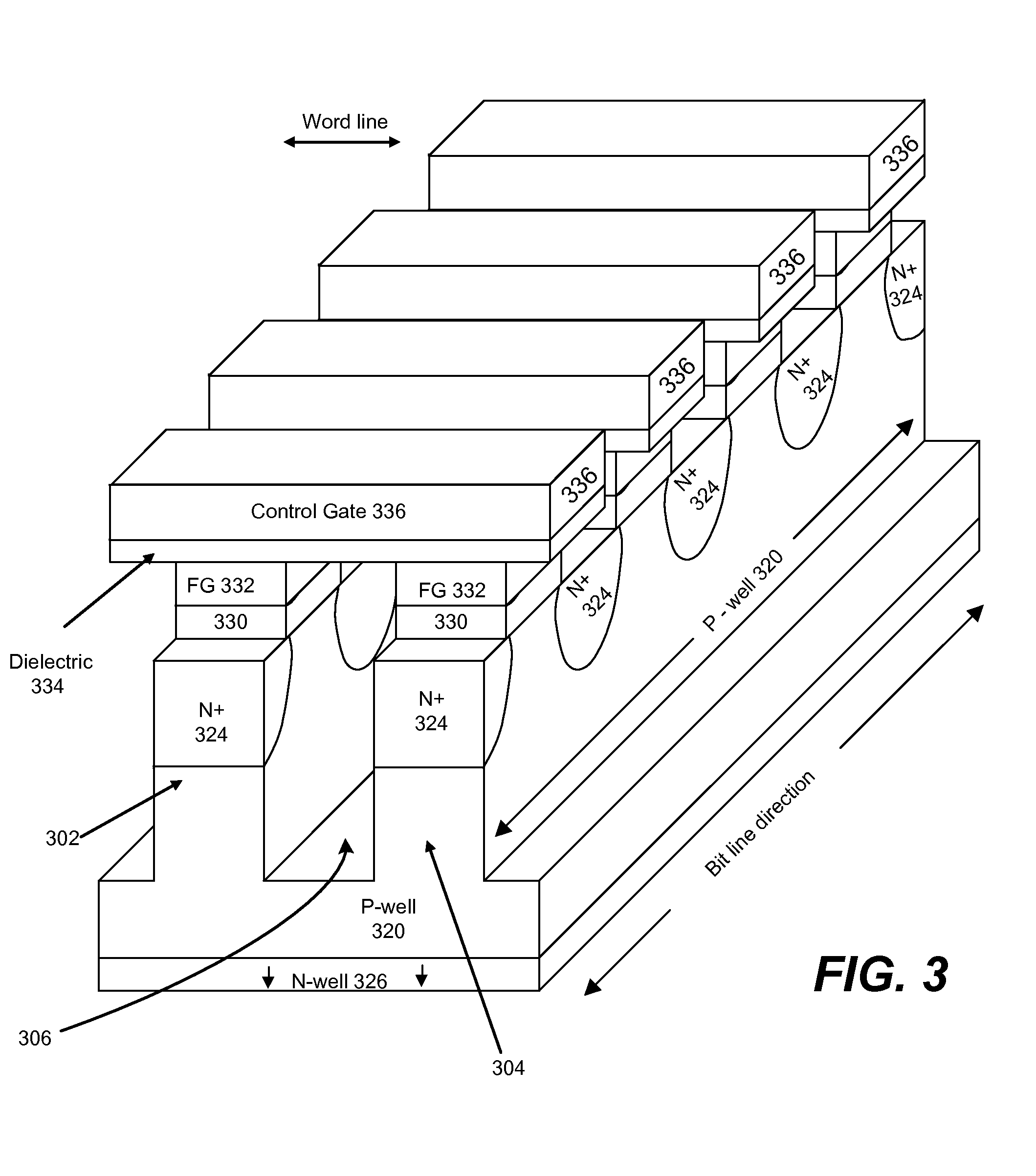
[0023]Embodiments in accordance with the present disclosure can be used in the formation of numerous types of high density semiconductor devices. A spacer and corresponding formation technique are provided to reduce the size of the fabricated elements. While not so limited, the described techniques can achieve feature sizes that are smaller than the smallest lithographically resolvable element size of the process being used. This can facilitate the high density formation of numerous types of elements in integrated semiconductor device fabrication. Various features and techniques are presented with respect to the NAND flash memory architecture. It will be appreciated from the provided disclosure that implementations of the disclosed technology are not so limited. By way of non-limiting example, embodiments in accordance with the present disclosure can provide and be used in the fabrication of a wide range of semiconductor devices, including but not limited to logic arrays, volatile m...


PUM


Abstract

High density semiconductor devices and methods of fabricating the same are provided. Spacer fabrication techniques are utilized to form circuit elements having reduced feature sizes, which in some instances are smaller than the smallest lithographically resolvable element size of the process being used. Spacers are formed that serve as a mask for etching one or more layers beneath the spacers. An etch stop pad layer having a material composition substantially similar to the spacer material is provided between a dielectric layer and an insulating sacrificial layer such as silicon nitride. When etching the sacrificial layer, the matched pad layer provides an etch stop to avoid damaging and reducing the size of the dielectric layer. The matched material compositions further provide improved adhesion for the spacers, thereby improving the rigidity and integrity of the spacers.

Description

CLAIM OF PRIORITY[0001]This application is a continuation application of U.S. patent application Ser. No. 11 / 623,315, entitled “SPACER PATTERNS USING ASSIST LAYER FOR HIGH DENSITY SEMICONDUCTOR DEVICES,” filed Jan. 15, 2007, which is incorporated herein by reference in its entirety.CROSS-REFERENCE TO RELATED APPLICATION[0002]The following application is cross-referenced and incorporated by reference herein in its entirety:[0003]U.S. patent application Ser. No. 11 / 623,314, entitled “Method of Forming Spacer Patterns Using Assist Layer for High Density Semiconductor Devices,” by James Kai, et al., filed on even date herewith.BACKGROUND OF THE INVENTION[0004]1. Field of the Invention[0005]Embodiments of the present disclosure are directed to high density semiconductor devices, such as non-volatile memory, and methods of forming the same.[0006]2. Description of the Related Art[0007]In most integrated circuit applications, there is continual pressure to shrink the substrate area required...

Claims


Application Information

Patent Timeline
Patent Type & Authority Applications(United States)
IPC IPC(8): H01L21/336
CPCH01L27/115H01L27/11524H01L27/11521H10B69/00H10B41/30H10B41/35
Inventor KAI, JAMESMATAMIS, GEORGEPHAM, TUAN DUCHIGASHITANI, MASAAKIORIMOTO, TAKASHI
Owner WODEN TECH INC
Why Eureka
Try Eureka