Semiconductor wafer with improved crack protection

a technology of semiconductor wafers and crack protection, which is applied in the direction of semiconductor devices, semiconductor/solid-state device details, electrical devices, etc., can solve the problems of crack propagation through dies, crack propagation can severely damage, or at the very least degrade, the resultant integrated circui

Inactive Publication Date: 2008-07-31
NXP USA INC
View PDF12 Cites 22 Cited by
  • Summary
  • Abstract
  • Description
  • Claims
  • Application Information

AI Technical Summary

Problems solved by technology

During the dicing process, the dicing tool can induce stresses on the semiconductor wafer that can lead to crack propagation through the dies.
Crack propagation can severely damage, or at the very least degrade, the resultant integrated circuit.
However, as with the other prior methods described earlier, the semiconductor wafer disclosed in US 2005 / 0266661 does not address the problem of dicing tool induced interlayer delamination between the layers deposited onto the silicon substrate.

Method used


Image

  • Semiconductor wafer with improved crack protection
  • Semiconductor wafer with improved crack protection
  • Semiconductor wafer with improved crack protection

Examples


fourth embodiment

[0057]FIG. 9 depicts another partial view of a semiconductor wafer 900 in accordance with the present invention. The embodiment illustrated in FIG. 9 is similar to the embodiment illustrated in FIG. 7 and FIG. 8. However, in this embodiment the ends of the trenches 316, 706 are shaped to promote point-to-point crack propagation between the ends of the trenches 316-n, 704-n (where n=1 to 4). In the present case, the ends of the trenches 316, 706 are tapered and terminate at an acuate head. The acuate head provides a stress point for concentrating dicing tool induced stresses and thus provides a point where crack propagation is more likely to initiate. In addition, because each of the consecutive trenches includes an acuate head, crack propagation is diverted between the head of the consecutive trenches of the same line of trenches, as is depicted in FIG. 10.

[0058]As will be appreciated, although the embodiment illustrated in FIG. 9 includes trenches having ends that taper inwardly fr...

fifth embodiment

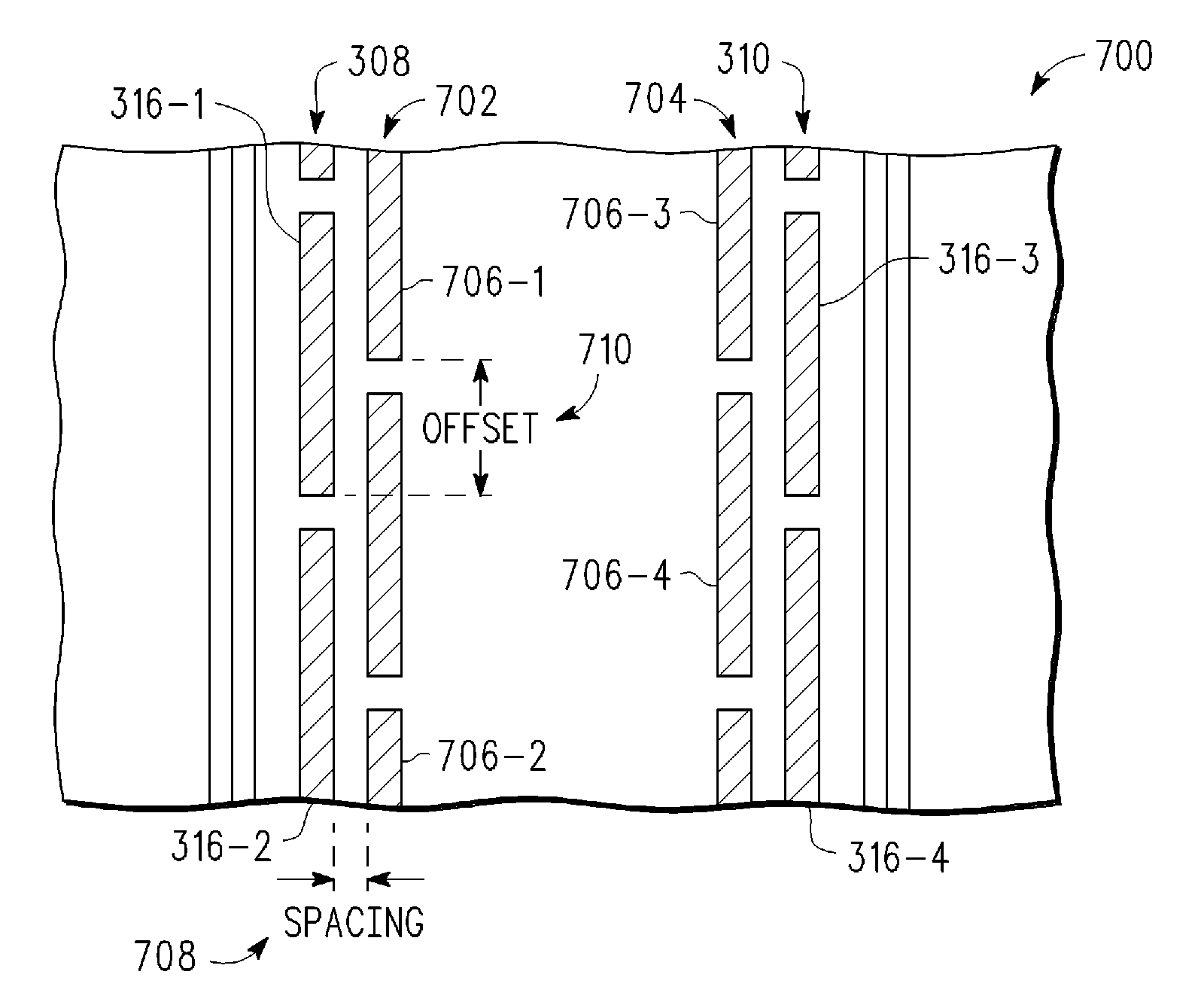
[0059]FIG. 11 depicts a partial top view of a semiconductor wafer 1100 in accordance with the present invention. The embodiment illustrated in FIG. 11 includes a combination of lines 308, 310 comprising trenches 316 of the type described with reference to FIGS. 3A and 4A, combined with a second pair of lines 702, 704 lines of trenches 706 of the type described with reference to FIG. 9.

[0060]As will be appreciated, other combinations may also be formed without departing from the scope of the present invention. In this embodiment, the lines 702, 704 of trenches 706 provides an initial protection mechanism to divert dicing tool induced crack propagation through the gaps 602. The lines 308, 310 comprising trenches 316 provide a secondary protection mechanism that buffers the die area 200 from dicing tool induced stresses and thus further reduces the susceptibility of the semiconductor wafer 1100 from resultant damage or degradation. As will be appreciated, the depicted first pair of lin...


PUM


Abstract

A method of manufacturing a semiconductor wafer for dicing includes providing a semiconductor wafer including a substrate and a plurality of upper layers on the substrate that form a formation of die areas. The formation is arranged so that adjacent die areas are separated by a path for a dicing tool within each path, a pair of spaced apart lines is fabricated. Each line defines a dicing edge of a respective path and has at least one trench extending between a top surface of the wafer and the substrate. Each trench is filled with a stress absorbing material for reducing die tool induced stress on the die areas during dicing.

Description

BACKGROUND OF THE INVENTION[0001]The present invention relates generally to the manufacture of semiconductor wafers and more particularly, to a method of manufacturing semiconductor wafers that include protection from die tool induced crack propagation.[0002]An individual integrated circuit or chip is usually formed from a larger structure known as a semiconductor wafer, which is usually comprised primarily of silicon, although other materials such as gallium arsenide and indium phosphide may be used. The semiconductor wafer includes a plurality of integrated circuits arranged in rows and columns with the periphery of each integrated circuit typically being square or rectangular in shape.[0003]Typically, after fabrication the semiconductor wafer is sawn or “diced” into square or rectangular shaped discrete integrated circuits along two mutually perpendicular sets of parallel lines or streets lying between each of the rows and columns of integrated circuits. The singulated integrated...

Claims


Application Information

Patent Timeline
Patent Type & Authority Applications(United States)
IPC IPC(8): H01L23/544H01L21/76
CPCH01L21/3043H01L21/312H01L21/78H01L23/562H01L2924/0002H01L23/585H01L2924/00H01L21/02118
Inventor YIP, HENG KEONGLO, WAI YEWTAN, LAN CHU
Owner NXP USA INC
Why Eureka
Try Eureka