Mugfet circuit for increasing output resistance

Active Publication Date: 2008-12-11
INFINEON TECH AG
View PDF7 Cites 8 Cited by
  • Summary
  • Abstract
  • Description
  • Claims
  • Application Information

AI Technical Summary

Problems solved by technology

This adversely affects carrier mobility and junction capacitance.
Moreover, the multiple gate configuration provides for greater control of the conducting channel and reduces detrimental pe

Method used


Image

  • Mugfet circuit for increasing output resistance
  • Mugfet circuit for increasing output resistance
  • Mugfet circuit for increasing output resistance

Examples


Example

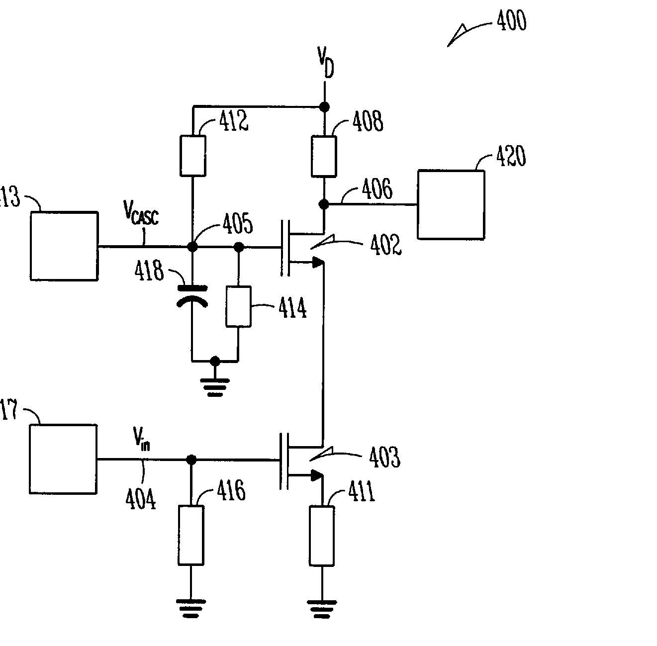
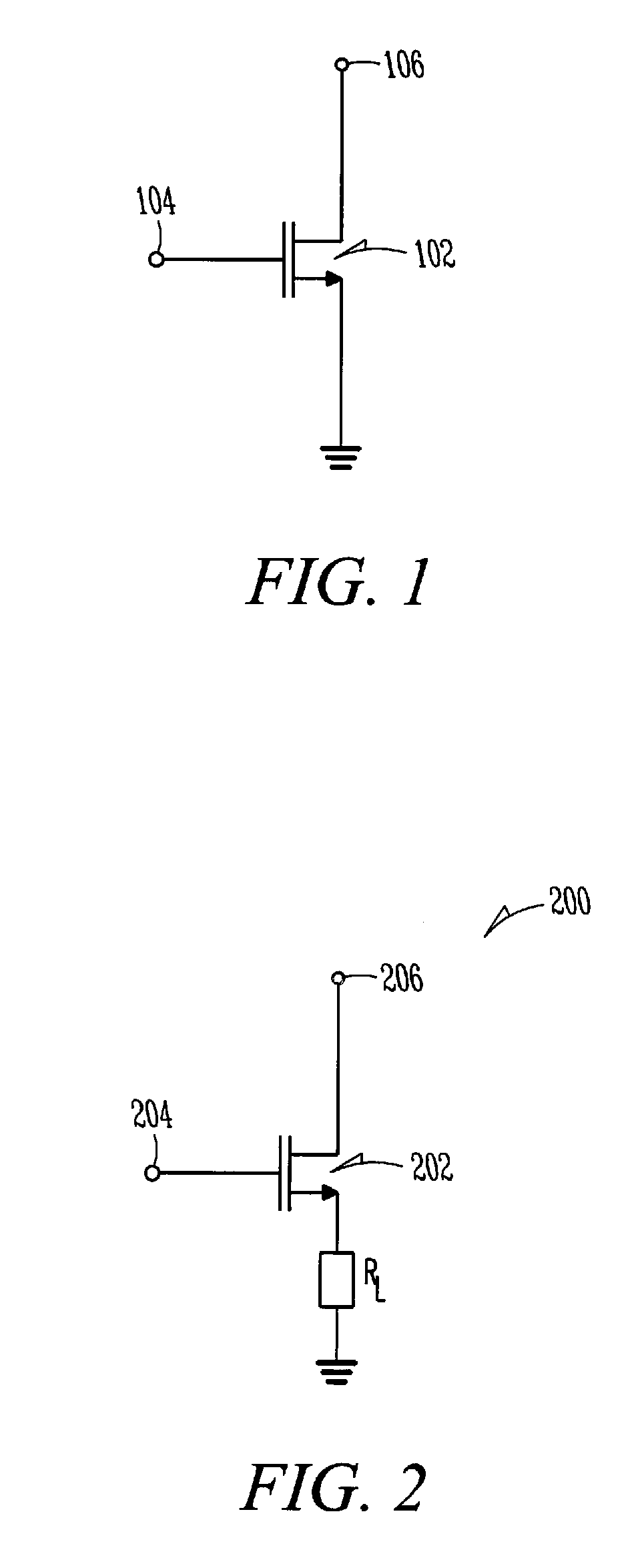
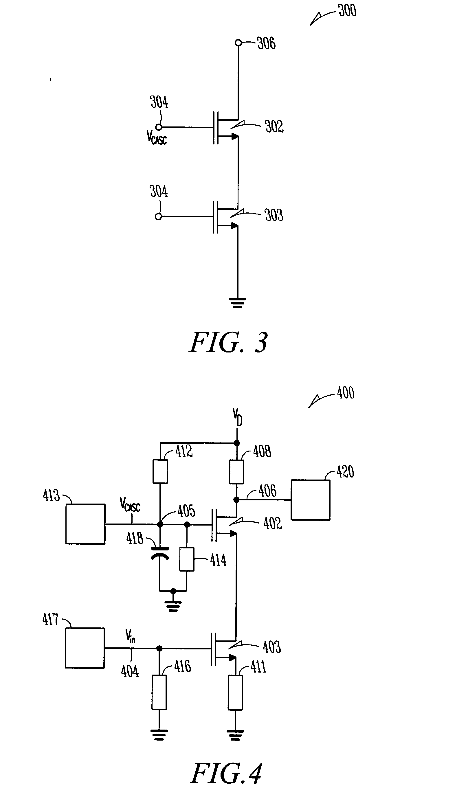
[0008]The following detailed description refers to the accompanying drawings that show, by way of illustration, specific details and embodiments in which the invention may be practiced. These embodiments are described in sufficient detail to enable those skilled in the art to practice the invention. Other embodiments may be utilized and structural, logical, and electrical changes may be made without departing from the scope of the invention. The various embodiments are not necessarily mutually exclusive, as some embodiments can be combined with one or more other embodiments to form new embodiments.

[0009]In the following description, the terms “wafer” and “substrate” may be used interchangeably to refer generally to any structure on which integrated circuits are formed and also to such structured during various stages of integrated circuit fabrication. The term “substrate” is understood to include a semiconductor wafer. The term “substrate” is also used to refer to semiconductor stru...


PUM


Abstract

In an embodiment, an apparatus includes a MuGFET device coupled to a reference source, the MuGFET device configured to receive an input signal at a gate thereof; and Also includes a further MuGFET device coupled between the MuGFET device and a first terminal of a load, a second terminal of the load coupled to a further reference source, the further MuGFET device configured to receive a further input signal at a gate thereof, and wherein the MuGFET device and the further MuGFET device are disposed above a substrate and configured to provide an output signal at the first terminal of the load.

Description

TECHNICAL FIELD[0001]Various embodiments described herein relate to semiconductor devices and, more particularly, to field effect transistors.BACKGROUND[0002]Multi-gate field effect transistor devices are often designed for applications with scaled-down extremely small devices which operate at low supply voltages. Moreover, multi-gate devices have gates on multiple sides of the conducting channel thereby providing better control of the semiconductor device.BRIEF DESCRIPTION OF THE DRAWINGS[0003]FIG. 1 is a schematic view of a conventional MuGFET circuit.[0004]FIG. 2 is a schematic view of a conventional MuGFET circuit;[0005]FIG. 3 is a schematic view of a multiple MuGFET circuit according to some embodiments of the invention;[0006]FIG. 4 is a more detailed schematic view of the MuGFET circuit of FIG. 3 connected according to some embodiments of the invention; and[0007]FIG. 5 is a simplified perspective view of the MuGFET circuit of FIG. 3, according to some embodiments of the invent...

Claims


Application Information

Patent Timeline
IPC IPC(8): H03F3/16H01L29/772
CPCH01L27/1203H01L29/785H03F1/22H03F3/16H03F3/50H03F2200/498H03F2200/513H01L27/1211
Inventor KNOBLINGER, GERHARD
Owner INFINEON TECH AG
Why Eureka
Try Eureka