Touch panel and display device using the same

a display device and touch panel technology, applied in the direction of gas-filled discharge tubes, electric discharge tubes, instruments, etc., can solve the problems of low sensitivity, accuracy and durability, low wearability/durability of metal electrode materials, and easy damage of electrodes formed on the substrate during operation,

Active Publication Date: 2009-06-18
TSINGHUA UNIV +1
View PDF98 Cites 95 Cited by
  • Summary
  • Abstract
  • Description
  • Claims
  • Application Information

AI Technical Summary

Benefits of technology

[0008]In operation, an upper surface of the touch panel is pressed / touched with a touch tool, such as a finger, or an electrical pen. And visual observation of a screen on the liquid crystal display device provided on a back side of the touch panel is allowed. In use, due to an electrical field of the user, a coupling capacitance forms between the user and the transparent conductive layer. For high frequency electrical current, the coupled capacitance is a conductor, thus the touch tool takes away a little current from the touch point. Current flowing through the four electrodes cooperatively replace the current lost at the touch point. The quantity of current supplied by the four electrodes is directly proportional to the distances from the touch point to the electrodes. A touch panel controller is used to calculate the proportion of the four supplied currents, thereby detecting coordinates of the touch point on the touch panel.

Problems solved by technology

However, the material of the electrodes such as metal has poor wearability / durability and low chemical endurance.
Further, when the substrate is deformable and made of soft material, the electrodes formed on the substrate is easily to be destroyed and break off during operation.
The above-mentioned problems of the metallic electrodes make for a touch panel with low sensitivity, accuracy and durability.
Additionally, the cost for forming the metallic electrodes is relatively high.

Method used


Image

  • Touch panel and display device using the same
  • Touch panel and display device using the same
  • Touch panel and display device using the same

Examples


Embodiment Construction

[0020]Reference will now be made to the drawings to describe, in detail, embodiments of the present touch panel and display device using the same.

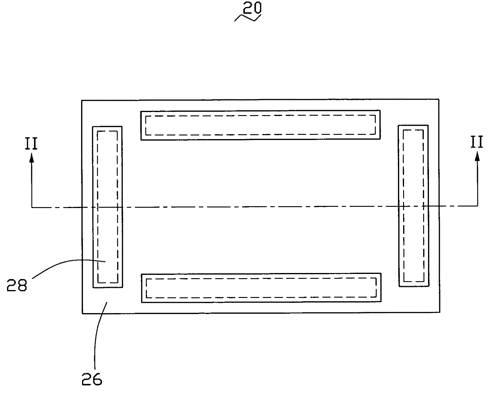
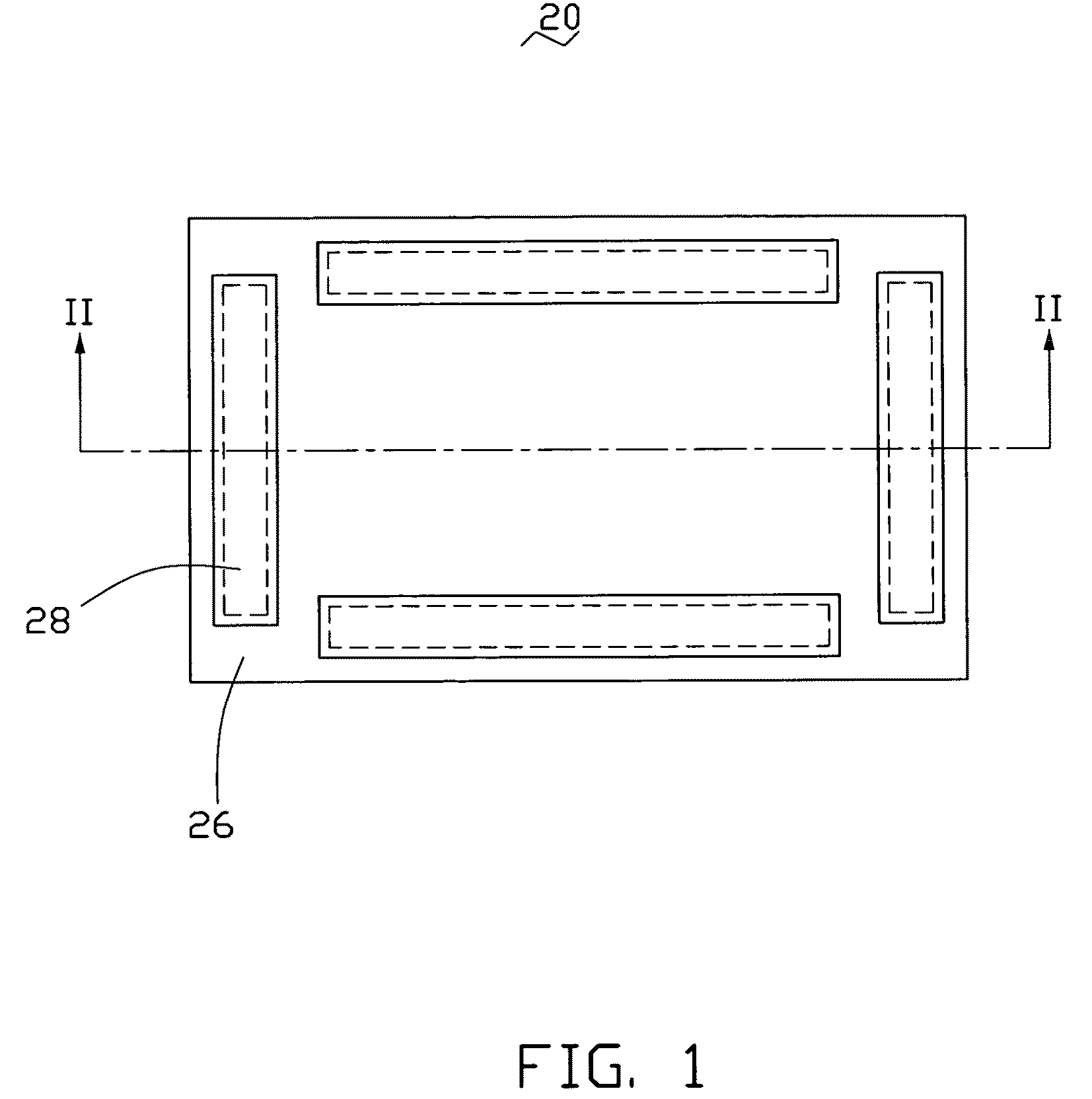
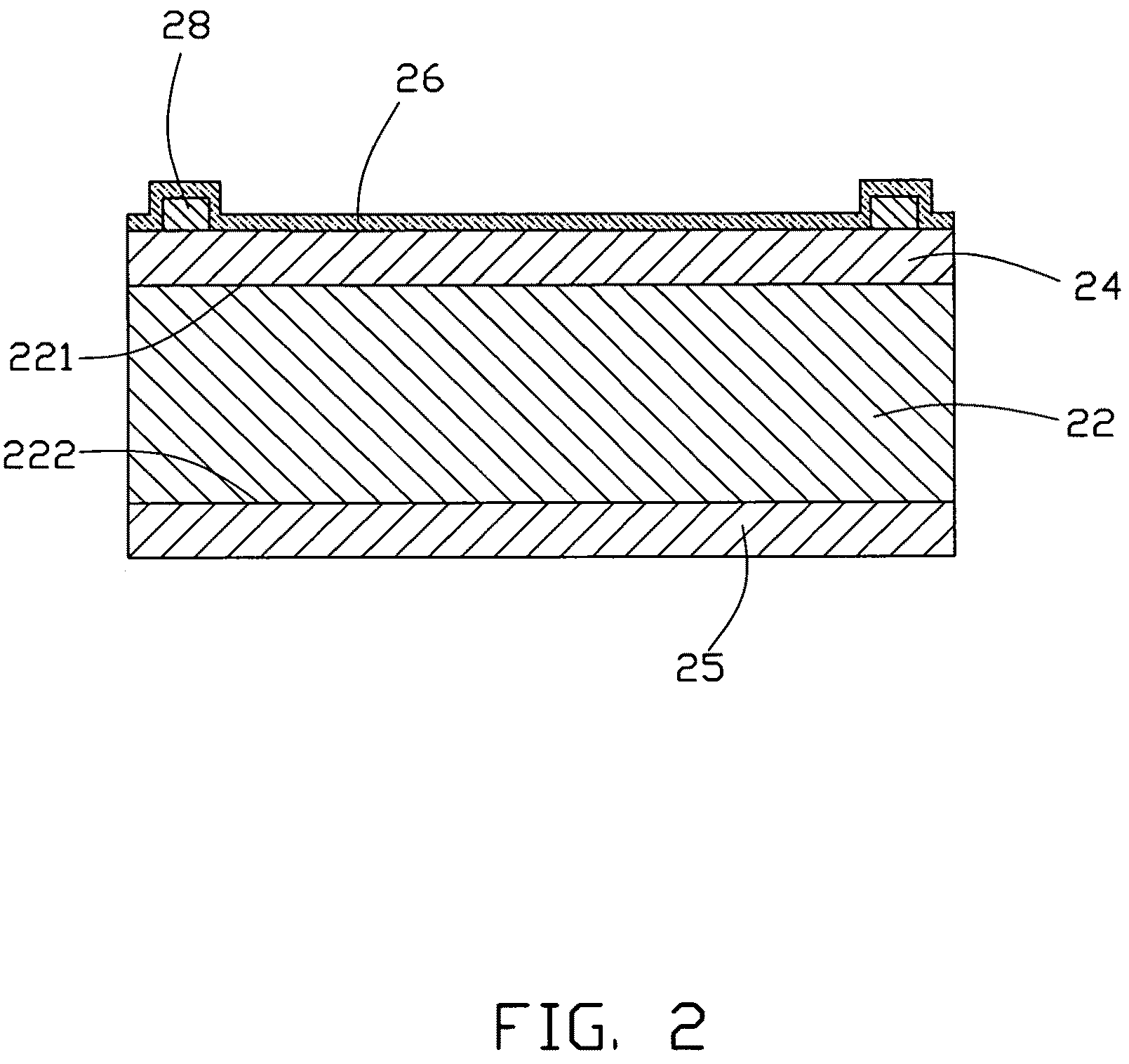
[0021]Referring to FIG. 1 and FIG. 2, a touch panel 20 includes a substrate 22, a transparent conductive layer 24, a protective layer 26, and at least two electrodes 28. The substrate 22 has a first surface 221 and a second surface 222 opposite to the first surface 221. The transparent conductive layer 24 is disposed on the first surface 221. The electrodes 28 are separately disposed on edges or corners of the transparent conductive layer 24 and electrically connected therewith for forming an equipotential surface on the transparent conductive layer 24. The transparent protective layer 26 covers the exposed surface of the transparent conductive layer 24 and the electrodes 28, away from the substrate 22.

[0022]It is to be noted that the shape of the substrate 22 and the transparent conductive layer 24 is chosen according to the requirements ...


PUM


Abstract

A touch panel includes a substrate, a transparent conductive layer, and at least two electrodes. The transparent conductive layer is disposed on the substrate. The at least two electrodes is separately disposed, and electrically connected with the transparent conductive layer. At least one of the electrodes includes a carbon nanotube layer. Further a display device using the above-described touch panel is also included.

Description

RELATED APPLICATIONS[0001]This application is related to commonly-assigned applications entitled, “TOUCH PANEL”, filed ______ (Atty. Docket No. US17449); “TOUCH PANEL”, filed ______ (Atty. Docket No. US17448); “TOUCH PANEL AND DISPLAY DEVICE USING THE SAME”, filed ______ (Atty. Docket No. US17889); “TOUCH PANEL AND DISPLAY DEVICE USING THE SAME”, filed ______ (Atty. Docket No. US17818); “TOUCH PANEL AND DISPLAY DEVICE USING THE SAME”, filed ______ (Atty. Docket No. US17820); “ELECTRONIC ELEMENT HAVING CARBON NANOTUBES”, filed ______ (Atty. Docket No. US18066); “TOUCH PANEL AND DISPLAY DEVICE USING THE SAME”, filed ______ (Atty. Docket No. US17862); “TOUCH PANEL AND DISPLAY DEVICE USING THE SAME”, filed ______ (Atty. Docket No. US17863); “TOUCH PANEL AND DISPLAY DEVICE USING THE SAME”, filed ______ (Atty. Docket No. US18263); “TOUCHABLE CONTROL DEVICE”, filed ______ (Atty. Docket No. US18262); “TOUCH PANEL AND DISPLAY DEVICE USING THE SAME”, filed ______ (Atty. Docket No. US17888); “...

Claims


Application Information

Patent Timeline
Patent Type & Authority Applications(United States)
IPC IPC(8): G06F3/041
CPCG06F3/044G06F3/0443
Inventor JIANG, KAI-LILIU, LIANGFAN, SHOU-SHAN
Owner TSINGHUA UNIV
Why Eureka
Try Eureka