Light emitting diode and manufacturing method thereof

a technology of light-emitting diodes and manufacturing methods, which is applied in the direction of semiconductor/solid-state device manufacturing, electrical equipment, semiconductor devices, etc., can solve the problem of preventing a uniform distribution of light over the light output surfa

Inactive Publication Date: 2010-01-07
HON HAI PRECISION IND CO LTD
View PDF2 Cites 4 Cited by
  • Summary
  • Abstract
  • Description
  • Claims
  • Application Information

AI Technical Summary

Benefits of technology

[0009]The present invention relates, in another aspect, to a method of manufacturing a light emitting diode. According to an exemplary embodiment of the present invention, the light emitting diode includes a substrate, a light emitting diode chip and an encapsulation unit. The substrate defines a receiving recess therein. The encapsulation unit disposed in the receiving recess and encapsulating the light emitting diode chip in the receiving recess. The encapsulation unit has a first encapsulation material and a second encapsulation material. The first encapsulation material is located over to the light emitting diode chip and the second encapsulation material is located around the first encapsulation material. The method includes the following steps: providing a mold which has a same configuration as the second encapsulation material, putting the mold in the receiving recess to occupy a first space of the receiving recess, and injecting a first mixture of a transparent colloid and a plurality of first particles into the receiving recess to fill a remaining second space of the receiving recess; solidifying the first mixture to form the first encapsulation material with the first particles distributed in the first encapsulation material with a first distributing density; removing the mold out of the receiving recess, and injecting a second mixture of a transparent colloid and a plurality of second particles into the first space of the receiving recess formed after the mold is removed out of the receiving recess; and solidifying the second mixture to form the second encapsulation material with the second particles distributed in the second encapsulation material with a second distributing density which is smaller than the first distributing density.

Problems solved by technology

The light is directly refracted by the light output surface of the encapsulation material, whose smooth nature can not help the majority of light to be dispersed to a periphery area of the light output surface to satisfy a requirement of uniform light illumination, without glare.
Thus, the majority of the light emitted from the LED chip leaves the LED from the encapsulation material as a beam, which causes the periphery area of the light output surface to be darker than the central area thereof, thereby preventing a uniform distribution of light over the light output surface.

Method used


Image

  • Light emitting diode and manufacturing method thereof
  • Light emitting diode and manufacturing method thereof
  • Light emitting diode and manufacturing method thereof

Examples


Embodiment Construction

[0015]Reference will now be made to the drawings to describe the various present embodiments in detail.

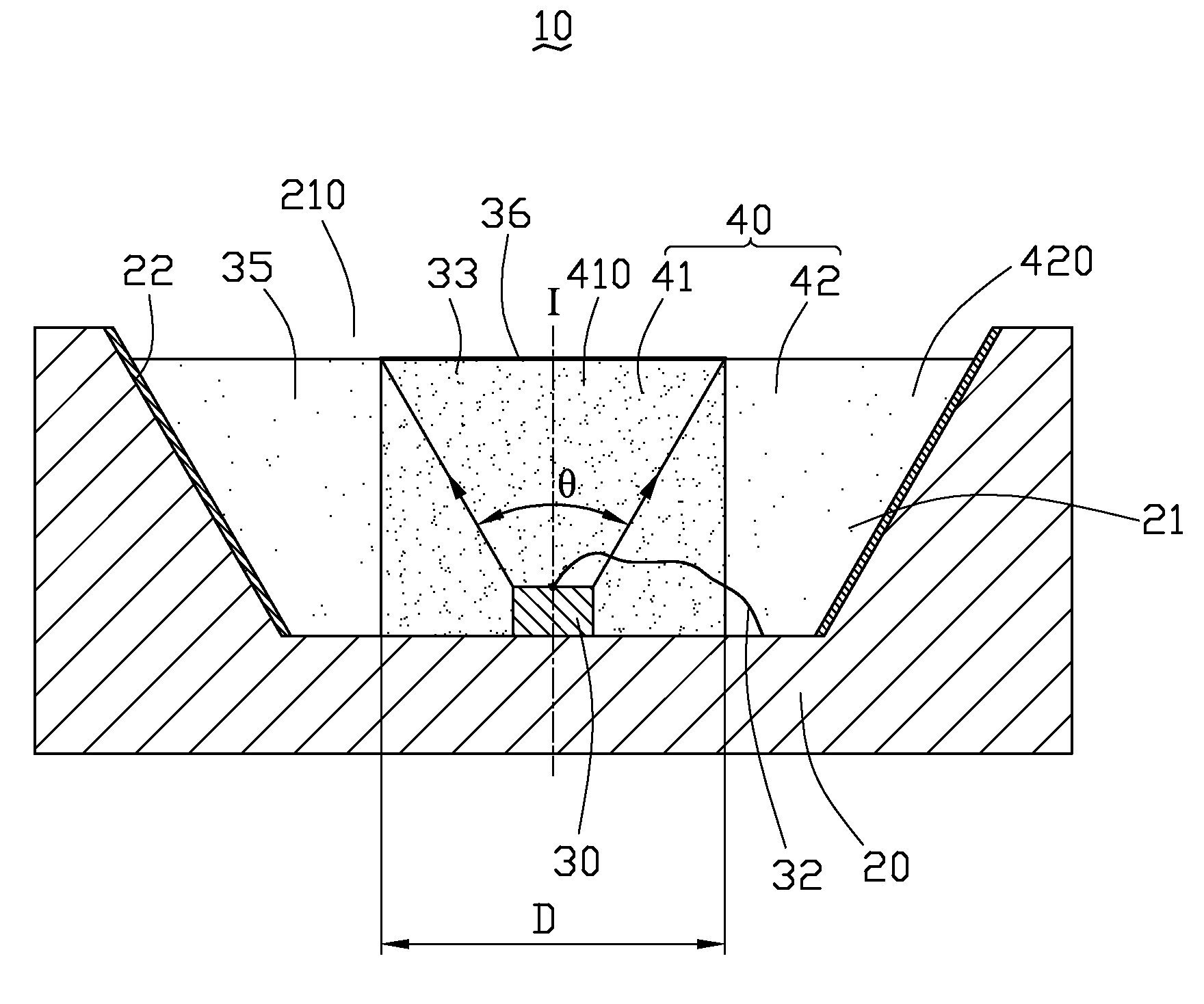
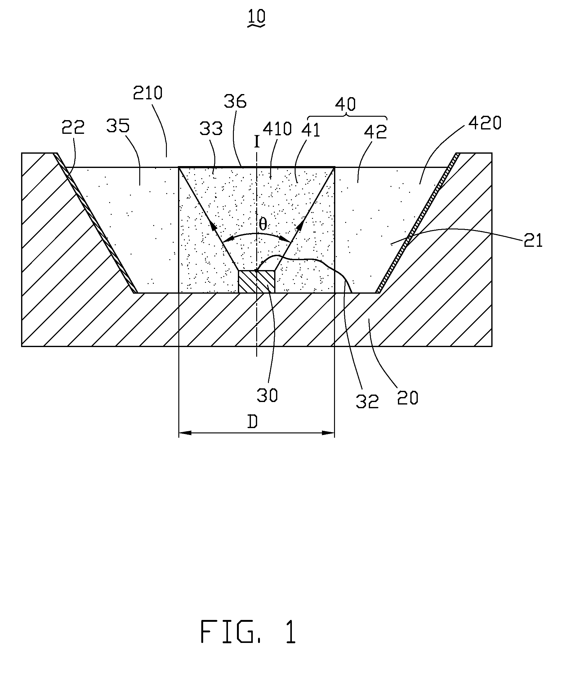
[0016]Referring to FIG. 1, a light emitting diode (LED) 10 includes a substrate 20, a LED chip 30, and an encapsulation unit 40.

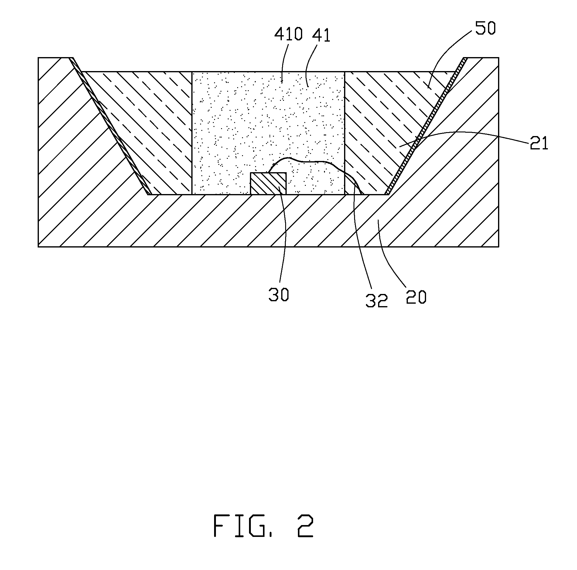
[0017]The substrate 20 defines a receiving recess 21 therein. The receiving recess 21 is concaved downwardly from a top surface of the substrate 20 towards a bottom surface of the substrate 20. The receiving recess 21 is bowl-shaped, and includes a bottom face paralleled to the top surface of the substrate 20 and an annular side face extending upwardly and outwardly from the bottom face towards the top surface of the substrate 20. A reflecting layer 22 is formed on the annular side face of the receiving recess 21 for reflecting light generated by the LED chip 30 and incident thereon towards a top opening 210 of the receiving recess 21. The LED chip 30 is electrically connected to the substrate 20 via a gold wire 32.

[0018]The encapsulation unit 40 includes ...


PUM


Abstract

An exemplary light emitting diode (LED) includes a substrate, a LED chip and an encapsulation unit. The encapsulation unit includes a first encapsulation material located over the LED chip and a second encapsulation material located around the first encapsulation material. A plurality of first particles with a first distributing density is distributed in the first encapsulation material. A plurality of second particles with a second distributing density is distributed in the second encapsulation material. The first distributing density is larger than the second distributing density, a central portion of light from the light emitting diode chip transmits through the first encapsulation material and exits the encapsulation unit from a top surface thereof, and a periphery portion of light from the light emitting diode chip transmits through the second encapsulation material and exits the encapsulation unit from the top surface thereof.

Description

BACKGROUND[0001]1. Field of the Invention[0002]The present invention relates to a light emitting diode and a manufacturing method thereof.[0003]2. Description of Related Art[0004]Currently, LEDs (light emitting diode) are preferred for use in non-emissive display devices rather than CCFLs (cold cathode fluorescent lamp) due to their high brightness, long lifespan, and wide color range.[0005]A related light emitting diode (LED) includes a LED chip and an encapsulation material encapsulating the LED chip therein. The encapsulation material has a planar top surface as a light output surface. In operation, light emitted from the LED chip shoots towards the encapsulation material, and leaves the LED from the light output surface of the encapsulation material.[0006]It is known that a majority of light from the LED chip travels towards a central area of the light output surface. The light is directly refracted by the light output surface of the encapsulation material, whose smooth nature c...

Claims


Application Information

Patent Timeline
Patent Type & Authority Applications(United States)
IPC IPC(8): H01L33/00H01L21/00
CPCH01L33/54H01L2933/0091H01L33/56H01L2224/45144H01L2224/48091H01L2924/00014H01L2924/00
Inventor CHANG, CHIA-SHOU
Owner HON HAI PRECISION IND CO LTD
Why Eureka
Try Eureka