Contactless power transmission circuit

a transmission circuit and contactless technology, applied in the direction of inductance, conversion with intermediate conversion to dc, process and machine control, etc., can solve the problems of increasing standby power and inability to accurately detect charging and non-charging, and achieve the effect of reducing standby power

Active Publication Date: 2010-07-08
PANASONIC CORP
View PDF14 Cites 78 Cited by
  • Summary
  • Abstract
  • Description
  • Claims
  • Application Information

AI Technical Summary

Benefits of technology

[0011]An object of the present invention is to provide a contactless power transmission circuit capable of reducing standby power.
[0012]One aspect of the present invention is directed to a contactless power transmission circuit for transmitting power in a contactless state to a power receiving device placed on a placing portion, comprising a resonant circuit including a power transmission coil for transmitting power to the power receiving device and a resonant capacitor which resonates with the power transmission coil; a switching element for resonating the resonant circuit by being repeatedly turned on and off; and a driving circuit for detecting whether or not the power receiving device is placed on the placing portion based on a voltage of the power transmission coil and driving the switching element such that an ON-period of the switching element is shorter when the power receiving device is detected not to be placed than when the power receiving device is placed.

Problems solved by technology

Thus, a current flowing into the power transmission coil increases, resulting in a problem of increasing standby power.
Since the input current is unstable by being influenced by the commercial power supply, there is a problem of being unable to accurately detect charging and non-charging.

Method used


Image

  • Contactless power transmission circuit
  • Contactless power transmission circuit
  • Contactless power transmission circuit

Examples


first embodiment

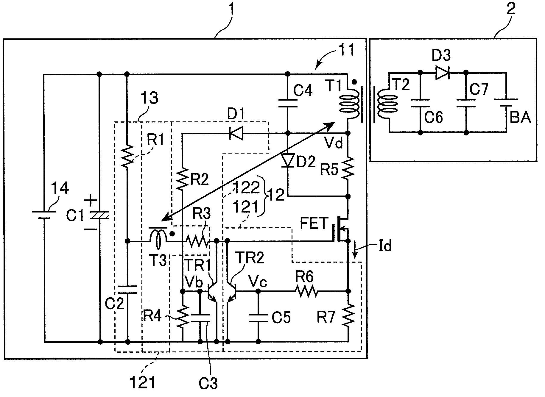
[0021]FIG. 1 is a circuit diagram of a charging system, to which a contactless power transmission circuit according to a first embodiment of the present invention is applied. This charging system is provided with a contactless power transmission circuit 1 and a power receiving device 2. The contactless power transmission circuit 1 is a charging circuit including a placing portion (not shown), on which the power receiving device 2 is to be placed, in a housing and adapted to charge the power receiving device 2 by transmitting power in a contactless manner to the power receiving device 2 placed on this placing portion. A rechargeable electric device such as an electric toothbrush, a mobile phone, a notebook personal computer, an electric shaver or an electric tool can be, for example, adopted as the power receiving device 2.

[0022]The contactless power transmission circuit 1 includes a resonant circuit 11, a switching element FET, a driving circuit 12, a bias circuit 13, a capacitor C1...

second embodiment

[0060]FIG. 4 is a circuit diagram of a charging system, to which a contactless power transmission circuit according to a second embodiment of the present invention is applied. The contactless power transmission circuit according to this embodiment is characterized by causing the separately-excited oscillation of a resonant circuit 11. In this embodiment, the same elements as those of the first embodiment are not described.

[0061]As shown in FIG. 4, a driving circuit 12 includes a microcomputer 100, a diode D1, resistors R2, R4 and a capacitor C3.

[0062]The microcomputer 100 includes a CPU, a ROM, a RAM, a dedicated hardware circuit and the like and outputs a PWM signal to a gate of a switching element FET from a PWM output port P3 to turn the switching element FET on and off by executing a control program stored in the ROM. A drive voltage VCC of 5 V output from a power supply 14 is input to a VCC port P2.

[0063]Here, the microcomputer 100 has the capacitor C3 connected between an AD i...

third embodiment

[0074]A contactless power transmission circuit 1 according to a third embodiment is characterizing by further providing a voltage regulator diode in the contactless power transmission circuit 1 of the first embodiment. FIG. 6 is a circuit diagram of a charging system, to which the contactless power transmission circuit 1 according to the third embodiment of the present invention is applied. In this embodiment, the same elements as those of the first and second embodiments are not described.

[0075]As shown in FIG. 6, a voltage regulator diode Z1 is provided between a resistor R2 and a diode D1. This voltage regulator diode Z1 is, for example, a Zener diode and an anode thereof is connected to the resistor R2 and a cathode thereof is connected to the diode D1.

[0076]The voltage regulator diode Z1 causes a current to flow from a resonant circuit 11 to a resistor R4 when a voltage of the cathode becomes larger than that of the anode by larger than a specified value while causing no curren...


PUM

PropertyMeasurementUnit
threshold voltageaaaaaaaaaa
drive voltageaaaaaaaaaa
voltageaaaaaaaaaa

Abstract

A driving circuit drives a switching element such that an ON-period of the switching element is shorter when a power receiving device is detected not to be placed than when the power receiving device is placed.

Description

BACKGROUND OF THE INVENTION AND RELATED ART STATEMENT[0001]1. Field of the Invention[0002]The present invention relates to a contactless power transmission circuit for transmitting power in a contactless manner to a power receiving device placed on a placing portion.[0003]2. Description of the Related Art[0004]In recent years, there has been known a contactless power transmission circuit provided with a resonant circuit including a power transmission coil for transmitting power to a power receiving device and a resonance coil which resonates with this power transmission coil, a switching elements for resonating this resonant circuit and a driving circuit for driving this switching element, and adapted to transmit power in a contactless manner to the power receiving device placed on a placing portion and charge the power receiving device (see, for example, patent literature 1 (Publication of JP No. 3416863), patent literature 2 (Publication of JP No. 3363341)).[0005]In such a contact...

Claims


Application Information

Patent Timeline
Patent Type & Authority Applications(United States)
IPC IPC(8): H01F38/00H02J7/00H02M3/28
CPCH02J7/025H02M3/3385H02J50/12Y10T307/944Y02B70/1433H02J50/10H02J50/90H02J7/00712Y02B70/10
Inventor KITAMURA, HIROYASUKADA, KYOHEI
Owner PANASONIC CORP
Why Eureka
Try Eureka