System and method of silicon switched power delivery using a package

a technology of switching power and package, applied in the direction of logic circuit, semiconductor/solid-state device details, pulse technique, etc., can solve the problems of increasing routing complexity, increasing power consumption of circuitry, and small circuitry, so as to reduce current leakage, simplify the placement of components on the substrate, and improve the effect of voltage level

Active Publication Date: 2007-11-15
QUALCOMM INC
View PDF29 Cites 18 Cited by
  • Summary
  • Abstract
  • Description
  • Claims
  • Application Information

AI Technical Summary

Benefits of technology

[0022] Another advantage is provided in that, by centralizing the power control and by removing the switches from the load circuit, component placement on the substrate is simplified, since it is no longer necessary to route input power to the component and it is no longer necessary to route multiple power grids over and around the distributed switch circuit.
[0023] Still another particular advantage is that the switch may be sized to meet a peak demand of the processing unit, where the peak demand of the processing unit is less than a peak power density multiplied by the substrate area of the processing unit.
[0024] An additional advantage includes decoupling of the load circuit designs from power switching, which allows the switch to be constructed of thicker oxide devices that have lower current leakage and that operate at higher voltage levels.
[0025] Another particular advantage is that the load circuit can be designed for performance without having to engineer a power switch into the design to reduce standby power.
[0026] Yet another advantage is that the peak demand of the total load circuit is lower than the peak power density multiplied by the area of the load circuit. Accordingly, while a distributed switch may be designed to meet the peak power density, the concentrated supply switch can meet the peak demand of the entire load circuit. The peak demand of the entire load circuit may be on an order of ½ to ⅓rd of the peak power density multiplied by the area of the load circuit. Therefore, the size of the switch can be reduced by the same order of magnitude, while maintaining the voltage loss of the distributed switches.
[0027] Still another advantage is that the current utilized to cycle the power switch can be reduced and better managed, since the physical size of the switch can be reduced to a fraction of the size of the distributed switch. Moreover, the switch may be activated in stages, making it easier to control the current level and to achieve a desired fraction of the output supply current at an output of the switch.

Problems solved by technology

Within such devices, the circuitry is becoming smaller, and power consumption by the circuitry is becoming increasingly significant to performance.
However, such designs increase routing complexity and decrease available area for component layout on the substrate.

Method used


Image

  • System and method of silicon switched power delivery using a package
  • System and method of silicon switched power delivery using a package
  • System and method of silicon switched power delivery using a package

Examples


Embodiment Construction

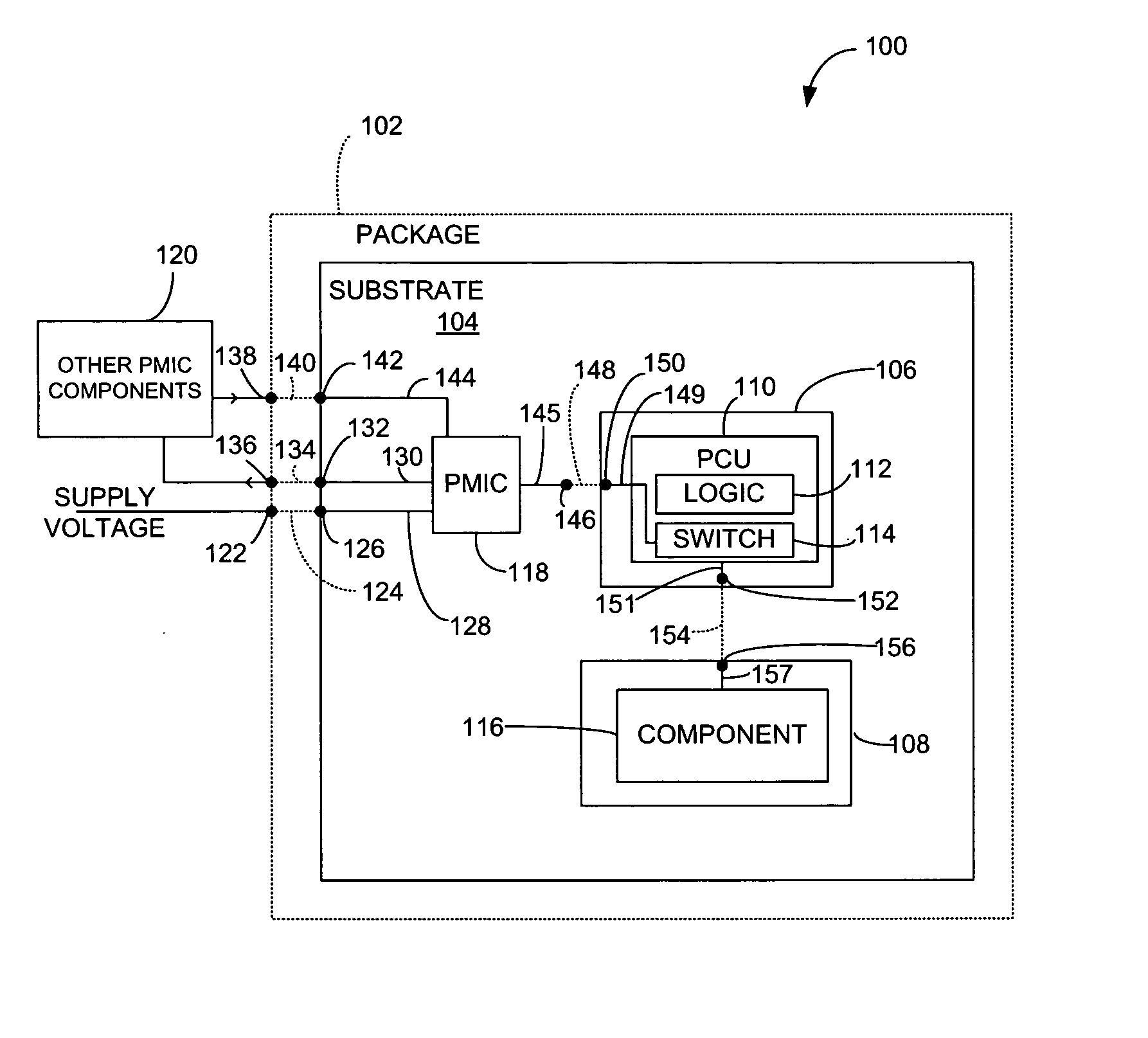
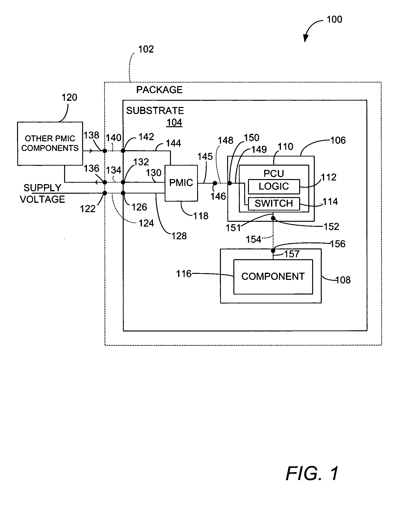
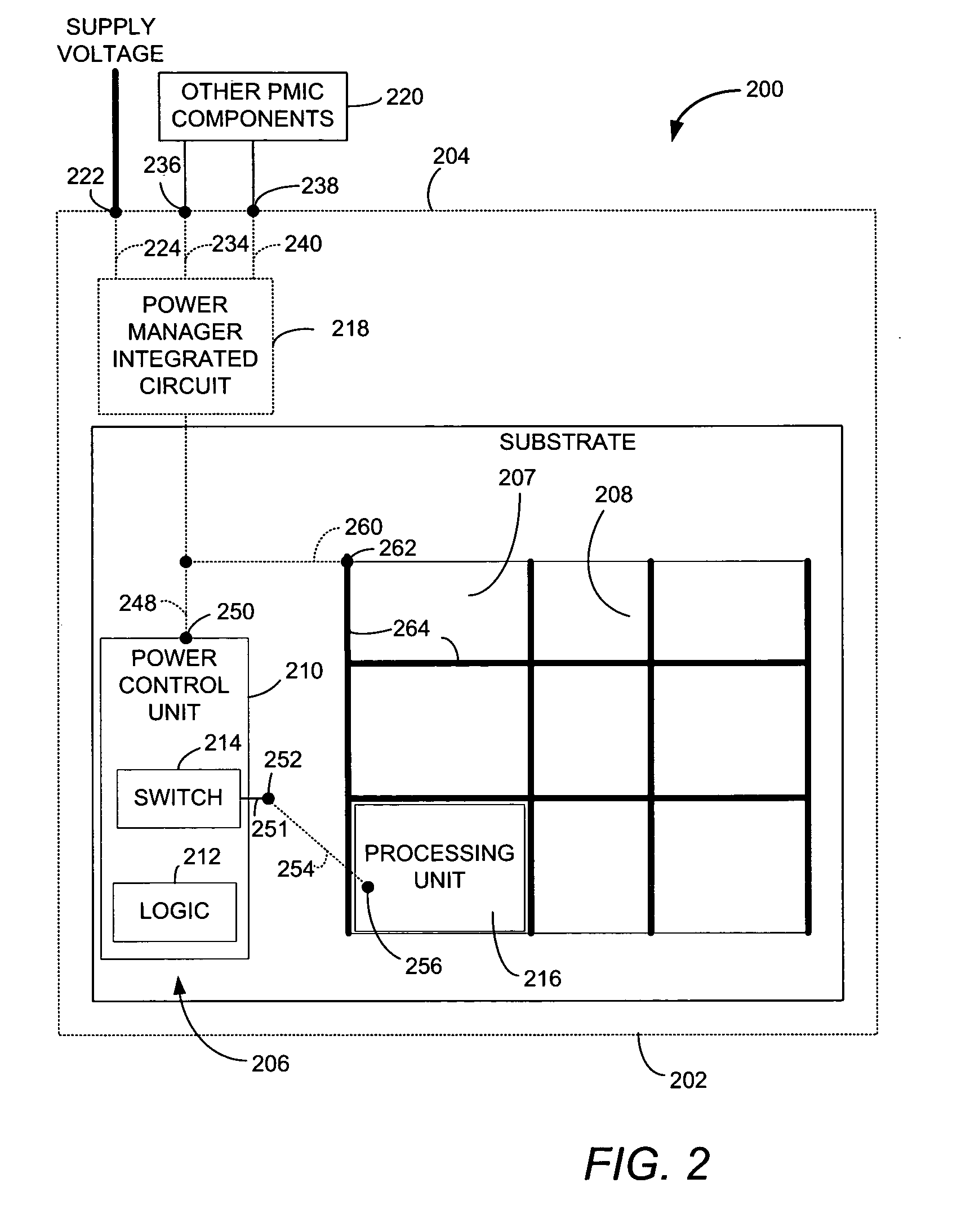
[0040] In a particular embodiment, a control unit within first domain of a substrate may utilize a metallization portion of an off-substrate package to selectively route power, signals, or a combination thereof to a second domain of the substrate that is electrically isolated from the first domain. The second domain may include, for example, an electrical component such as a processor, a memory, other integrated circuit resources, and the like. In integrated circuitry, the voltage efficiencies often have a significant impact overall performance. By routing power and signals through the off-substrate package, the control unit may reduce voltage loss by taking advantage of the metallization of the package, which typically has a lower electrical resistance than metal traces within the substrate. The control unit may route power or shut off power to selected components to activate or deactivate components of the substrate. In some instances, the activation and deactivation of components...


PUM


Abstract

In one particular embodiment, an integrated circuit includes a package and a substrate electrically and physically coupled to the package. The package includes a first pin, a second pin, and metallization coupling the first pin to the second pin. The substrate is coupled to the package via the first pin and the second pin. The substrate includes a plurality of power domains and a power control unit. The second pin of the package is coupled to a particular power domain of the plurality of power domains. The power control unit includes logic and a switch, where the switch includes a first terminal coupled to a voltage supply terminal, a control terminal coupled to the logic, and a second terminal coupled to the first pin of the package. The logic selectively activates the switch to distribute power to the particular power domain via the metallization of the package.

Description

BACKGROUND [0001] I. Field [0002] The present disclosure generally relates to systems and methods of power distribution in a circuit, and more particularly to systems and methods using low-resistance package metals to distribute switched power or signals to designated areas of a silicon substrate. [0003] II. Description of Related Art [0004] Advances in technology have resulted in smaller and more powerful personal computing devices. For example, a variety of portable personal computing devices, including wireless computing devices, such as portable wireless telephones, personal digital assistants (PDAs), and paging devices are small, lightweight, and easily carried by users. More specifically, portable wireless telephones, such as cellular (analog and digital) telephones and IP telephones, can communicate voice and data packets over wireless networks. Further, many such wireless telephones include other types of devices that are incorporated therein. For example, a wireless telepho...

Claims


Application Information

Patent Timeline
Patent Type & Authority Applications(United States)
IPC IPC(8): H01L23/52
CPCH03K17/223H01L2924/0002H01L2924/00H03K19/00
Inventor CHOA-EOAN, LEW G.TOMS, THOMAS R.ANDREEV, BORIS DIMITROVROSEN GAGNE, JUSTIN JOSEPHSHI, CHUNLEI
Owner QUALCOMM INC
Why Eureka
Try Eureka